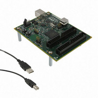
DK-DEV-5M570ZN Altera, DK-DEV-5M570ZN Datasheet - Page 126

DK-DEV-5M570ZN
Manufacturer Part Number
DK-DEV-5M570ZN
Description
KIT DEV MAX V 5M570Z
Manufacturer
Altera
Series
MAX® Vr
Type
CPLDr
Datasheets
1.DK-DEV-5M570ZN.pdf
(30 pages)
2.DK-DEV-5M570ZN.pdf
(2 pages)
3.DK-DEV-5M570ZN.pdf
(30 pages)
4.DK-DEV-5M570ZN.pdf
(164 pages)
5.DK-DEV-5M570ZN.pdf
(24 pages)
Specifications of DK-DEV-5M570ZN
Contents
Board, Cable(s), Software and Documentation
Silicon Manufacturer
Altera
Core Architecture
CPLD
Core Sub-architecture
MAX
Silicon Core Number
5M
Silicon Family Name
MAX V
Kit Contents
MAX V CPLD Development Board, USB Cable
Rohs Compliant
Yes
Lead Free Status / RoHS Status
Lead free / RoHS Compliant
For Use With/related Products
5M570ZF256
Lead Free Status / Rohs Status
Compliant
Other names
544-2722
Available stocks
Company
Part Number
Manufacturer
Quantity
Price
- DK-DEV-5M570ZN PDF datasheet
- DK-DEV-5M570ZN PDF datasheet #2
- DK-DEV-5M570ZN PDF datasheet #3
- DK-DEV-5M570ZN PDF datasheet #4
- DK-DEV-5M570ZN PDF datasheet #5
- Current page: 126 of 164
- Download datasheet (5Mb)
7–24
MAX V Device Handbook
The Quartus II software supports both the Base mode (uses 8-bit address and data)
and the Extended mode (uses 16-bit address and data). Base mode uses only UFM
sector 0 (2,048 bits), while Extended mode uses both UFM sector 0 and sector 1 (8,192
bits). There are only four pins in SPI: SI, SO, SCK, and nCS.
pins and functions.
Table 7–9. SPI Interface Signals
Data transmitted to the SI port of the slave device is sampled by the slave device at
the positive SCK clock. Data transmits from the slave device through SO at the negative
SCK clock edge. When nCS is asserted, it means the current device is being selected by
the master device from the other end of the SPI bus for service. When nCS is not
asserted, the SI and SCK ports should be blocked from receiving signals from the
master device, and SO should be in High Impedance state to avoid causing contention
on the shared SPI bus. All instructions, addresses, and data are transferred with the
MSB first and start with high-to-low nCS transition. The circuit diagram is shown in
Figure
Figure 7–20. Circuit Diagram for SPI Interface Read or Write Operations
SI
SO
SCK
nCS
Pin
7–20.
UFM Block
Serial Data Input
Serial Data Output
Serial Data Clock
Chip Select
Description
Receive data serially.
Transmit data serially.
The clock signal produced from the master device to
synchronize the data transfer.
Active low signal that enables the slave device to
receive or transfer data from the master device.
Eight-Bit Status Shift Register
Read, Write, and Erase
Address and Data Hub
Op-Code Decoder
Chapter 7: User Flash Memory in MAX V Devices
State Machine
Table 7–9
Function
January 2011 Altera Corporation
Software Support for UFM Block
describes the SPI
Control Logic
SPI Interface
SI SO SCK nCS
Related parts for DK-DEV-5M570ZN
Image
Part Number
Description
Manufacturer
Datasheet
Request
R

Part Number:
Description:
KIT DEV ARRIA II GX FPGA 2AGX125
Manufacturer:
Altera
Datasheet:

Part Number:
Description:
KIT DEV CYCLONE III LS EP3CLS200
Manufacturer:
Altera
Datasheet:

Part Number:
Description:
KIT DEV STRATIX IV FPGA 4SE530
Manufacturer:
Altera
Datasheet:

Part Number:
Description:
KIT DEV FPGA 2AGX260 W/6.375G TX
Manufacturer:
Altera
Datasheet:

Part Number:
Description:
KIT DEV STRATIX V FPGA 5SGXEA7
Manufacturer:
Altera
Datasheet:

Part Number:
Description:
KIT DEVELOPMENT STRATIX III
Manufacturer:
Altera
Datasheet:

Part Number:
Description:
KIT DEVELOPMENT STRATIX IV
Manufacturer:
Altera
Datasheet:

Part Number:
Description:
KIT DEV ARRIA GX 1AGX60N
Manufacturer:
Altera
Datasheet:

Part Number:
Description:
KIT STARTER CYCLONE IV GX
Manufacturer:
Altera
Datasheet:

Part Number:
Description:
KIT DEVELOPMENT STRATIX IV
Manufacturer:
Altera
Datasheet:

Part Number:
Description:
CPLD, EP610 Family, ECMOS Process, 300 Gates, 16 Macro Cells, 16 Reg., 16 User I/Os, 5V Supply, 35 Speed Grade, 24DIP
Manufacturer:
Altera Corporation
Datasheet:

Part Number:
Description:
CPLD, EP610 Family, ECMOS Process, 300 Gates, 16 Macro Cells, 16 Reg., 16 User I/Os, 5V Supply, 15 Speed Grade, 24DIP
Manufacturer:
Altera Corporation
Datasheet:


