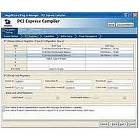
IPR-PCIE/1 Altera, IPR-PCIE/1 Datasheet - Page 171
IPR-PCIE/1
Manufacturer Part Number
IPR-PCIE/1
Description
IP CORE Renewal Of IP-PCIE/1
Manufacturer
Altera
Type
MegaCorer
Specifications of IPR-PCIE/1
Software Application
IP CORE, Interface And Protocols, PCI
Supported Families
Arria GX, Cyclone II, HardCopy II, Stratix II
Core Architecture
FPGA
Core Sub-architecture
Arria, Cyclone, Stratix
Rohs Compliant
NA
Function
PCI Express Compiler, x1 Link Width
License
Renewal License
Lead Free Status / RoHS Status
na
Lead Free Status / RoHS Status
na


Chapter 7: Reset and Clocks
Clocks
December 2010 Altera Corporation
Clocking for a Generic PIPE PHY and the Simulation Testbench
■
Figure 7–8
also used for the simulation testbench. As this figure illustrates the 100 MHz reference
clock drives the input to a PLL which creates a 125 MHz clock for the application
logic. For Gen1 operation, a 250 MHz clock drives the PCI Express IP core clock,
pclk_in. In Gen1 mode, clk500_out and rate_ext can be left unconnected. For Gen2
operation, clk500_out drives pclk_in.
Figure 7–8. Clocking for the Generic PIPE Interface and the Simulation Testbench, All Families
Note to
(1) Refer to
When you implement a generic PIPE PHY in the IP core, you must provide a 125 MHz
clock on the clk125_in input. Typically, the generic PIPE PHY provides the 125 MHz
clock across the PIPE interface.
All of the IP core interfaces, including the user application interface and the PIPE
interface, are synchronous to the clk125_in input. You are not required to use the
refclk and clk125_out signals in this case.
100 MHz Reference Clock and 125 MHz Application Clock
When implementing the Arria GX, Cyclone IV GX, HardCopy IV GX, Stratix II GX,
Stratix IV GX PHY, or Stratix V GX in a ×1 or ×4 configuration, or the Arria II GX in a
×1, ×4, or ×8 configuration, the 100 MHz clock is connected directly to the transceiver.
The clk125_out is driven by the output of the transceiver.
The clk125_out must be connected back to the clk125_in input, possibly through a
clock distribution circuit required by the specific application. The user application
interface is synchronous to the clk125_in input.
clk250_in – This signal is the clock for all of the ×8 IP core registers. All
synchronous application layer interface signals are synchronous to this clock.
clk250_in must be 250 MHz and it must be the exact same frequency as
clk250_out.
Clock Source
100-MHz
Figure
Table 7–1 on page 7–10
illustrates the clocking for a generic PIPE interface. The same clocking is
7–8:
<variant> .v or .vhd
refclk
to determine the required frequencies for various configurations.
pclk_in
pll_inclk
(PCIe MegaCore Function)
<variant> _core.v or .vhd
PLL
core_clk_out
clk125_out
clk250_out
Note 1
PCI Express Compiler User Guide
Application Clock
7–11
Related parts for IPR-PCIE/1
Image
Part Number
Description
Manufacturer
Datasheet
Request
R

Part Number:
Description:
IP CORE Renewal Of IP-PCI/MT32
Manufacturer:
Altera
Datasheet:
Part Number:
Description:
IP CORE Renewal Of IP-PCI/MT64
Manufacturer:
Altera
Datasheet:
Part Number:
Description:
IP CORE Renewal Of IP-PCI/T32
Manufacturer:
Altera
Datasheet:
Part Number:
Description:
IP CORE Renewal Of IP-PCI/T64
Manufacturer:
Altera
Datasheet:

Part Number:
Description:
IP CORE Renewal Of IP-PCIE/4
Manufacturer:
Altera
Datasheet:
Part Number:
Description:
IP CORE Renewal Of IP-PCIE/8
Manufacturer:
Altera
Datasheet:
Part Number:
Description:
IP NIOS II MEGACORE RENEW
Manufacturer:
Altera
Datasheet:
Part Number:
Description:
IP CORE Renewal Of IP-XAUIPCS
Manufacturer:
Altera
Datasheet:

Part Number:
Description:
CPLD, EP610 Family, ECMOS Process, 300 Gates, 16 Macro Cells, 16 Reg., 16 User I/Os, 5V Supply, 35 Speed Grade, 24DIP
Manufacturer:
Altera Corporation
Datasheet:
Part Number:
Description:
CPLD, EP610 Family, ECMOS Process, 300 Gates, 16 Macro Cells, 16 Reg., 16 User I/Os, 5V Supply, 15 Speed Grade, 24DIP
Manufacturer:
Altera Corporation
Datasheet:
Part Number:
Description:
Manufacturer:
Altera Corporation
Datasheet: