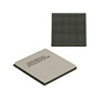
EP4SGX530HH35C2N Altera, EP4SGX530HH35C2N Datasheet - Page 1050

EP4SGX530HH35C2N
Manufacturer Part Number
EP4SGX530HH35C2N
Description
IC STRATIX IV FPGA 530K 1152HBGA
Manufacturer
Altera
Series
Stratix® IV GXr
Datasheets
1.EP4SGX110DF29C3N.pdf
(80 pages)
2.EP4SGX110DF29C3N.pdf
(1154 pages)
3.EP4SGX110DF29C3N.pdf
(432 pages)
4.EP4SGX110DF29C3N.pdf
(22 pages)
5.EP4SGX110DF29C3N.pdf
(30 pages)
6.EP4SGX110DF29C3N.pdf
(72 pages)
7.EP4SGX530HH35C2N.pdf
(1145 pages)
Specifications of EP4SGX530HH35C2N
Number Of Logic Elements/cells
531200
Number Of Labs/clbs
21248
Total Ram Bits
27376
Number Of I /o
564
Voltage - Supply
0.87 V ~ 0.93 V
Mounting Type
Surface Mount
Operating Temperature
0°C ~ 85°C
Package / Case
1152-HBGA
Family Name
Stratix® IV
Number Of Logic Blocks/elements
531200
# Registers
424960
# I/os (max)
560
Process Technology
40nm
Operating Supply Voltage (typ)
900mV
Logic Cells
531200
Ram Bits
28033024
Operating Supply Voltage (min)
0.87V
Operating Supply Voltage (max)
0.93V
Operating Temp Range
0C to 85C
Operating Temperature Classification
Commercial
Mounting
Surface Mount
Pin Count
1152
Package Type
FCHBGA
Lead Free Status / RoHS Status
Lead free / RoHS Compliant
Number Of Gates
-
Lead Free Status / Rohs Status
Compliant
Available stocks
Company
Part Number
Manufacturer
Quantity
Price
- EP4SGX110DF29C3N PDF datasheet
- EP4SGX110DF29C3N PDF datasheet #2
- EP4SGX110DF29C3N PDF datasheet #3
- EP4SGX110DF29C3N PDF datasheet #4
- EP4SGX110DF29C3N PDF datasheet #5
- EP4SGX110DF29C3N PDF datasheet #6
- EP4SGX530HH35C2N PDF datasheet #7
- Current page: 1050 of 1145
- Download datasheet (29Mb)
2–36
Phase 3—Compilation
Phase 4—Simulating the Design
Document Revision History
Table 2–7. Document Revision History
Stratix IV Device Handbook Volume 3
November 2009, v4.0
June 2009, v3.1
March 2009, v3.0
Date and Document Version
Create Data Processing and Other User Logic
For this example, you must implement the 8B/10B encoder and decoder in the FPGA
fabric.
and the system logic controls for all channels in the FPGA fabric. This block diagram
is a representation of a typical system and may not exactly show the different blocks
in a practical application. Interface all the logic blocks with the transceiver.
If you would like to add SignalTap for verification, first complete synthesis, then add
the transceiver-FPGA fabric or other user logic signals in SignalTap. Lastly, compile
the design to generate the .sof.
Assign pins for the input and output signals in your design. The Quartus II software
versions 8.1 and earlier do not allow pin assignments for the Stratix IV GX device.
Set the OCT values for the transceiver serial pins, add timing constraints for the clocks
and data paths in your logic, then compile the design.
To simulate the design, follow the steps outlined in
page
Table 2–7
2–12.
Figure 2–17 on page 2–35
shows the revision history for this chapter.
■
■
■
■
■
■
■
■
Added
Table
Minor text edits.
Updated the “Introduction”, “Power Supplies”,
“Transceiver Configuration”, “Clocking”, “Create
Transceiver Instances”, “Create Dynamic
Reconfiguration Controller Instances”, “Create
Data Processing and Other User Logic”,
“Functional Simulation” sections.
Added the “Board Design Requirements”, “Gear
Boxing Logic”, “Guidelines to Debug the FPGA
Logic and the Transceiver Interface”, and
“Guidelines to Debug System
sections.
Added introductory sentences to improve search
ability.
Add “Power Supplies” on page 2–6
Updated “Dynamic Reconfiguration” on page 2–4
Text edits
2–6.
Table
2–3,
Changes Made
Table
shows the logic on the transmitter and receiver side
2–4,
Table
Level
2–5, and
Issues”
“Functional Simulation” on
Chapter 2: Transceiver Design Flow Guide
© November 2009 Altera Corporation
Summary of Changes
Document Revision History
—
—
—
Related parts for EP4SGX530HH35C2N
Image
Part Number
Description
Manufacturer
Datasheet
Request
R

Part Number:
Description:
CYCLONE II STARTER KIT EP2C20N
Manufacturer:
Altera
Datasheet:

Part Number:
Description:
CPLD, EP610 Family, ECMOS Process, 300 Gates, 16 Macro Cells, 16 Reg., 16 User I/Os, 5V Supply, 35 Speed Grade, 24DIP
Manufacturer:
Altera Corporation
Datasheet:

Part Number:
Description:
CPLD, EP610 Family, ECMOS Process, 300 Gates, 16 Macro Cells, 16 Reg., 16 User I/Os, 5V Supply, 15 Speed Grade, 24DIP
Manufacturer:
Altera Corporation
Datasheet:

Part Number:
Description:
Manufacturer:
Altera Corporation
Datasheet:

Part Number:
Description:
CPLD, EP610 Family, ECMOS Process, 300 Gates, 16 Macro Cells, 16 Reg., 16 User I/Os, 5V Supply, 30 Speed Grade, 24DIP
Manufacturer:
Altera Corporation
Datasheet:

Part Number:
Description:
High-performance, low-power erasable programmable logic devices with 8 macrocells, 10ns
Manufacturer:
Altera Corporation
Datasheet:

Part Number:
Description:
High-performance, low-power erasable programmable logic devices with 8 macrocells, 7ns
Manufacturer:
Altera Corporation
Datasheet:

Part Number:
Description:
Classic EPLD
Manufacturer:
Altera Corporation
Datasheet:

Part Number:
Description:
High-performance, low-power erasable programmable logic devices with 8 macrocells, 10ns
Manufacturer:
Altera Corporation
Datasheet:

Part Number:
Description:
Manufacturer:
Altera Corporation
Datasheet:

Part Number:
Description:
Manufacturer:
Altera Corporation
Datasheet:

Part Number:
Description:
Manufacturer:
Altera Corporation
Datasheet:

Part Number:
Description:
CPLD, EP610 Family, ECMOS Process, 300 Gates, 16 Macro Cells, 16 Reg., 16 User I/Os, 5V Supply, 25 Speed Grade, 24DIP
Manufacturer:
Altera Corporation
Datasheet:


