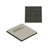
EP4SGX530HH35C2N Altera, EP4SGX530HH35C2N Datasheet - Page 598

EP4SGX530HH35C2N
Manufacturer Part Number
EP4SGX530HH35C2N
Description
IC STRATIX IV FPGA 530K 1152HBGA
Manufacturer
Altera
Series
Stratix® IV GXr
Datasheets
1.EP4SGX110DF29C3N.pdf
(80 pages)
2.EP4SGX110DF29C3N.pdf
(1154 pages)
3.EP4SGX110DF29C3N.pdf
(432 pages)
4.EP4SGX110DF29C3N.pdf
(22 pages)
5.EP4SGX110DF29C3N.pdf
(30 pages)
6.EP4SGX110DF29C3N.pdf
(72 pages)
7.EP4SGX530HH35C2N.pdf
(1145 pages)
Specifications of EP4SGX530HH35C2N
Number Of Logic Elements/cells
531200
Number Of Labs/clbs
21248
Total Ram Bits
27376
Number Of I /o
564
Voltage - Supply
0.87 V ~ 0.93 V
Mounting Type
Surface Mount
Operating Temperature
0°C ~ 85°C
Package / Case
1152-HBGA
Family Name
Stratix® IV
Number Of Logic Blocks/elements
531200
# Registers
424960
# I/os (max)
560
Process Technology
40nm
Operating Supply Voltage (typ)
900mV
Logic Cells
531200
Ram Bits
28033024
Operating Supply Voltage (min)
0.87V
Operating Supply Voltage (max)
0.93V
Operating Temp Range
0C to 85C
Operating Temperature Classification
Commercial
Mounting
Surface Mount
Pin Count
1152
Package Type
FCHBGA
Lead Free Status / RoHS Status
Lead free / RoHS Compliant
Number Of Gates
-
Lead Free Status / Rohs Status
Compliant
Available stocks
Company
Part Number
Manufacturer
Quantity
Price
- EP4SGX110DF29C3N PDF datasheet
- EP4SGX110DF29C3N PDF datasheet #2
- EP4SGX110DF29C3N PDF datasheet #3
- EP4SGX110DF29C3N PDF datasheet #4
- EP4SGX110DF29C3N PDF datasheet #5
- EP4SGX110DF29C3N PDF datasheet #6
- EP4SGX530HH35C2N PDF datasheet #7
- Current page: 598 of 1145
- Download datasheet (29Mb)
1–160
Figure 1–125. Rate Match Deletion in XAUI Mode
Stratix IV Device Handbook Volume 2
rx_rmfifodatadeleted
dataout[3]
dataout[2]
dataout[1]
dataout[0]
datain[3]
datain[2]
datain[1]
datain[0]
K28.5
K28.5
K28.5
K28.5
K28.5
K28.5
K28.5
K28.5
Rate Match FIFO
In XAUI mode, the rate match FIFO is capable of compensating for up to ±100 PPM
(200 PPM total) difference between the upstream transmitter and the local receiver
reference clock. The XAUI protocol requires the transmitter to send /R/ (/K28.0/)
code groups simultaneously on all four lanes (denoted as ||R|| column) during
inter-packet gaps, adhering to rules listed in the IEEE P802.3ae specification. The rate
match FIFO operation in XAUI mode is compliant to the IEEE P802.3ae specification.
The rate match operation begins after:
■
■
The rate match FIFO looks for the ||R|| column (simultaneous /R/ code group on
all four channels) and deletes or inserts ||R|| column to prevent the rate match FIFO
from overflowing or under-running. The rate match FIFO can insert or delete as many
||R|| columns as necessary to perform the rate match operation.
Two flags, rx_rmfifodatadeleted and rx_rmfifodatainserted, indicating
rate match FIFO deletion and insertion events, respectively, are forwarded to the
FPGA fabric. If an ||R|| column is deleted, the rx_rmfifodeleted flag from each
of the four channels goes high for one clock cycle per deleted ||R|| column. If an
||R|| column is inserted, the rx_rmfifoinserted flag from each of the four
channels goes high for one clock cycle per inserted ||R|| column.
Figure 1–125
columns are required to be deleted.
For more information, refer to
The synchronization state machine in the word aligner of all four channels
indicates synchronization has been acquired by driving the rx_syncstatus
signal high
The deskew FIFO indicates alignment has been acquired by driving the
rx_channelaligned signal high
K28.3
K28.3
K28.3
K28.3
K28.3
K28.3
K28.3
K28.3
shows an example of rate match deletion in the case where three ||R||
K28.5
K28.5
K28.5
K28.5
K28.5
K28.5
K28.5
K28.5
First ||R||
Column
K28.5
K28.5
K28.5
K28.5
K28.0
K28.0
K28.0
K28.0
“Rate Match FIFO in XAUI Mode” on page
K28.0
K28.0
K28.0
K28.0
K28.5
K28.5
K28.5
K28.5
Second ||R||
Column
K28.5
K28.5
K28.5
K28.5
K28.0
K28.0
K28.0
K28.0
Chapter 1: Stratix IV Transceiver Architecture
Third ||R||
Column
K28.0
K28.0
K28.0
K28.0
© March 2010 Altera Corporation
Transceiver Block Architecture
Fourth ||R||
Column
K28.0
K28.0
K28.0
K28.0
1–77.
K28.5
K28.5
K28.5
K28.5
Related parts for EP4SGX530HH35C2N
Image
Part Number
Description
Manufacturer
Datasheet
Request
R

Part Number:
Description:
CYCLONE II STARTER KIT EP2C20N
Manufacturer:
Altera
Datasheet:

Part Number:
Description:
CPLD, EP610 Family, ECMOS Process, 300 Gates, 16 Macro Cells, 16 Reg., 16 User I/Os, 5V Supply, 35 Speed Grade, 24DIP
Manufacturer:
Altera Corporation
Datasheet:

Part Number:
Description:
CPLD, EP610 Family, ECMOS Process, 300 Gates, 16 Macro Cells, 16 Reg., 16 User I/Os, 5V Supply, 15 Speed Grade, 24DIP
Manufacturer:
Altera Corporation
Datasheet:

Part Number:
Description:
Manufacturer:
Altera Corporation
Datasheet:

Part Number:
Description:
CPLD, EP610 Family, ECMOS Process, 300 Gates, 16 Macro Cells, 16 Reg., 16 User I/Os, 5V Supply, 30 Speed Grade, 24DIP
Manufacturer:
Altera Corporation
Datasheet:

Part Number:
Description:
High-performance, low-power erasable programmable logic devices with 8 macrocells, 10ns
Manufacturer:
Altera Corporation
Datasheet:

Part Number:
Description:
High-performance, low-power erasable programmable logic devices with 8 macrocells, 7ns
Manufacturer:
Altera Corporation
Datasheet:

Part Number:
Description:
Classic EPLD
Manufacturer:
Altera Corporation
Datasheet:

Part Number:
Description:
High-performance, low-power erasable programmable logic devices with 8 macrocells, 10ns
Manufacturer:
Altera Corporation
Datasheet:

Part Number:
Description:
Manufacturer:
Altera Corporation
Datasheet:

Part Number:
Description:
Manufacturer:
Altera Corporation
Datasheet:

Part Number:
Description:
Manufacturer:
Altera Corporation
Datasheet:

Part Number:
Description:
CPLD, EP610 Family, ECMOS Process, 300 Gates, 16 Macro Cells, 16 Reg., 16 User I/Os, 5V Supply, 25 Speed Grade, 24DIP
Manufacturer:
Altera Corporation
Datasheet:


