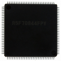
DF70844AD80FPV Renesas Electronics America, DF70844AD80FPV Datasheet - Page 275

DF70844AD80FPV
Manufacturer Part Number
DF70844AD80FPV
Description
IC SUPERH MCU FLASH 112LQFP
Manufacturer
Renesas Electronics America
Series
SuperH® SH7080r
Datasheet
1.DF70844AD80FPV.pdf
(1644 pages)
Specifications of DF70844AD80FPV
Core Size
32-Bit
Program Memory Size
256KB (256K x 8)
Core Processor
SH-2
Speed
80MHz
Connectivity
EBI/EMI, FIFO, I²C, SCI, SSU
Peripherals
DMA, POR, PWM, WDT
Number Of I /o
76
Program Memory Type
FLASH
Ram Size
16K x 8
Voltage - Supply (vcc/vdd)
3 V ~ 5.5 V
Data Converters
A/D 8x10b
Oscillator Type
Internal
Operating Temperature
-40°C ~ 85°C
Package / Case
112-LQFP
No. Of I/o's
76
Ram Memory Size
16KB
Cpu Speed
80MHz
Digital Ic Case Style
LQFP
Supply Voltage Range
3V To 3.6V, 4.5V To 5.5V
Embedded Interface Type
I2C, SCI
Rohs Compliant
Yes
Lead Free Status / RoHS Status
Lead free / RoHS Compliant
For Use With
R0K570865S001BE - KIT STARTER FOR SH7086R0K570865S000BE - KIT STARTER FOR SH7086HS0005KCU11H - EMULATOR E10A-USB H8S(X),SH2(A)
Eeprom Size
-
Lead Free Status / RoHS Status
Lead free / RoHS Compliant, Lead free / RoHS Compliant
Available stocks
Company
Part Number
Manufacturer
Quantity
Price
Company:
Part Number:
DF70844AD80FPV
Manufacturer:
Renesas Electronics America
Quantity:
10 000
- Current page: 275 of 1644
- Download datasheet (10Mb)
The bus state controller (BSC) outputs control signals for various types of memory that is
connected to the external address space and external devices. BSC functions enable this LSI to
connect directly with SRAM, SDRAM, and other memory storage devices, and external devices.
9.1
1. External address space
• A maximum 64 Mbytes for each of eight areas, CS0 to CS7, and a maximum 1 Gbyte for the
• Can specify the normal space interface, SRAM interface with byte selection, burst ROM
• Can select the data bus width (8, 16, or 32 bits) for each address space
• Controls the insertion of the wait state for each address space.
• Controls the insertion of the wait state for each read access and write access
• Can set the independent idling cycle in the continuous access for five cases: read-write (in
2. Normal space interface
• Supports the interface that can directly connect to the SRAM
3. Burst ROM interface (clock asynchronous)
• High-speed access to the ROM that has the page mode function
4. MPX-I/O interface
• Directly connects peripheral LSIs with address/data multiplexing
5. SDRAM interface
• Can set the SDRAM up to 2 areas
• Multiplex output for row address/column address
• Efficient access by single read/single write
• High-speed access by bank-active mode
• Supports an auto-refresh and self-refresh
6. SRAM interface with byte selection
• Supports interfaces that can be connected directly to SRAM with byte selection
CS8 area
(clock synchronous or asynchronous), MPX-I/O, burst MPX-I/O, SDRAM, or PCMCIA for
each address space
same space/different space), read-read (in same space/different space), the first cycle is a write
access.
Features
Section 9 Bus State Controller (BSC)
Rev. 3.00 May 17, 2007 Page 217 of 1582
Section 9 Bus State Controller (BSC)
REJ09B0181-0300
Related parts for DF70844AD80FPV
Image
Part Number
Description
Manufacturer
Datasheet
Request
R

Part Number:
Description:
KIT STARTER FOR M16C/29
Manufacturer:
Renesas Electronics America
Datasheet:

Part Number:
Description:
KIT STARTER FOR R8C/2D
Manufacturer:
Renesas Electronics America
Datasheet:

Part Number:
Description:
R0K33062P STARTER KIT
Manufacturer:
Renesas Electronics America
Datasheet:

Part Number:
Description:
KIT STARTER FOR R8C/23 E8A
Manufacturer:
Renesas Electronics America
Datasheet:

Part Number:
Description:
KIT STARTER FOR R8C/25
Manufacturer:
Renesas Electronics America
Datasheet:

Part Number:
Description:
KIT STARTER H8S2456 SHARPE DSPLY
Manufacturer:
Renesas Electronics America
Datasheet:

Part Number:
Description:
KIT STARTER FOR R8C38C
Manufacturer:
Renesas Electronics America
Datasheet:

Part Number:
Description:
KIT STARTER FOR R8C35C
Manufacturer:
Renesas Electronics America
Datasheet:

Part Number:
Description:
KIT STARTER FOR R8CL3AC+LCD APPS
Manufacturer:
Renesas Electronics America
Datasheet:

Part Number:
Description:
KIT STARTER FOR RX610
Manufacturer:
Renesas Electronics America
Datasheet:

Part Number:
Description:
KIT STARTER FOR R32C/118
Manufacturer:
Renesas Electronics America
Datasheet:

Part Number:
Description:
KIT DEV RSK-R8C/26-29
Manufacturer:
Renesas Electronics America
Datasheet:

Part Number:
Description:
KIT STARTER FOR SH7124
Manufacturer:
Renesas Electronics America
Datasheet:

Part Number:
Description:
KIT STARTER FOR H8SX/1622
Manufacturer:
Renesas Electronics America
Datasheet:

Part Number:
Description:
KIT DEV FOR SH7203
Manufacturer:
Renesas Electronics America
Datasheet:


