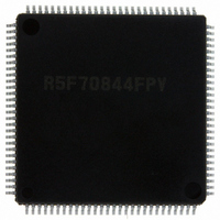
DF70844AD80FPV Renesas Electronics America, DF70844AD80FPV Datasheet - Page 627

DF70844AD80FPV
Manufacturer Part Number
DF70844AD80FPV
Description
IC SUPERH MCU FLASH 112LQFP
Manufacturer
Renesas Electronics America
Series
SuperH® SH7080r
Datasheet
1.DF70844AD80FPV.pdf
(1644 pages)
Specifications of DF70844AD80FPV
Core Size
32-Bit
Program Memory Size
256KB (256K x 8)
Core Processor
SH-2
Speed
80MHz
Connectivity
EBI/EMI, FIFO, I²C, SCI, SSU
Peripherals
DMA, POR, PWM, WDT
Number Of I /o
76
Program Memory Type
FLASH
Ram Size
16K x 8
Voltage - Supply (vcc/vdd)
3 V ~ 5.5 V
Data Converters
A/D 8x10b
Oscillator Type
Internal
Operating Temperature
-40°C ~ 85°C
Package / Case
112-LQFP
No. Of I/o's
76
Ram Memory Size
16KB
Cpu Speed
80MHz
Digital Ic Case Style
LQFP
Supply Voltage Range
3V To 3.6V, 4.5V To 5.5V
Embedded Interface Type
I2C, SCI
Rohs Compliant
Yes
Lead Free Status / RoHS Status
Lead free / RoHS Compliant
For Use With
R0K570865S001BE - KIT STARTER FOR SH7086R0K570865S000BE - KIT STARTER FOR SH7086HS0005KCU11H - EMULATOR E10A-USB H8S(X),SH2(A)
Eeprom Size
-
Lead Free Status / RoHS Status
Lead free / RoHS Compliant, Lead free / RoHS Compliant
Available stocks
Company
Part Number
Manufacturer
Quantity
Price
Company:
Part Number:
DF70844AD80FPV
Manufacturer:
Renesas Electronics America
Quantity:
10 000
- Current page: 627 of 1644
- Download datasheet (10Mb)
14. Output Waveform Control at Synchronous Counter Clearing in Complementary PWM Mode
Negative phase
Positive phase
Setting the WRE bit in TWCR to 1 suppresses initial output when synchronous counter
clearing occurs in the Tb interval at the trough in complementary PWM mode and controls
abrupt change in duty cycle at synchronous counter clearing.
Initial output suppression is applicable only when synchronous clearing occurs in the Tb
interval at the trough as indicated by (10) or (11) in figure 11.56. When synchronous clearing
occurs outside that interval, the initial value specified by the OLS bits in TOCR is output.
Even in the Tb interval at the trough, if synchronous clearing occurs in the initial value output
period (indicated by (1) in figure 11.56) immediately after the counters start operation, initial
value output is not suppressed.
This function can be used in both the MTU2 and MTU2S. In the MTU2, synchronous clearing
generated in channels 0 to 2 in the MTU2 can cause counter clearing in complementary PWM
mode; in the MTU2S, compare match or input capture flag setting in channels 0 to 2 in the
MTU2 can cause counter clearing.
Counter start
TGRA_3
TGRB_3
H'0000
TCDR
TDDR
Tb interval
(1)
Figure 11.56 Timing for Synchronous Counter Clearing
(2)
(3)
(4)
Tb interval
(5)
(6)
(7)
Section 11 Multi-Function Timer Pulse Unit 2 (MTU2)
(8)
(9)
Rev. 3.00 May 17, 2007 Page 569 of 1582
Tb interval
(10) (11)
Output waveform is active-low
TCNT_3
REJ09B0181-0300
TCNT_4
Related parts for DF70844AD80FPV
Image
Part Number
Description
Manufacturer
Datasheet
Request
R

Part Number:
Description:
KIT STARTER FOR M16C/29
Manufacturer:
Renesas Electronics America
Datasheet:

Part Number:
Description:
KIT STARTER FOR R8C/2D
Manufacturer:
Renesas Electronics America
Datasheet:

Part Number:
Description:
R0K33062P STARTER KIT
Manufacturer:
Renesas Electronics America
Datasheet:

Part Number:
Description:
KIT STARTER FOR R8C/23 E8A
Manufacturer:
Renesas Electronics America
Datasheet:

Part Number:
Description:
KIT STARTER FOR R8C/25
Manufacturer:
Renesas Electronics America
Datasheet:

Part Number:
Description:
KIT STARTER H8S2456 SHARPE DSPLY
Manufacturer:
Renesas Electronics America
Datasheet:

Part Number:
Description:
KIT STARTER FOR R8C38C
Manufacturer:
Renesas Electronics America
Datasheet:

Part Number:
Description:
KIT STARTER FOR R8C35C
Manufacturer:
Renesas Electronics America
Datasheet:

Part Number:
Description:
KIT STARTER FOR R8CL3AC+LCD APPS
Manufacturer:
Renesas Electronics America
Datasheet:

Part Number:
Description:
KIT STARTER FOR RX610
Manufacturer:
Renesas Electronics America
Datasheet:

Part Number:
Description:
KIT STARTER FOR R32C/118
Manufacturer:
Renesas Electronics America
Datasheet:

Part Number:
Description:
KIT DEV RSK-R8C/26-29
Manufacturer:
Renesas Electronics America
Datasheet:

Part Number:
Description:
KIT STARTER FOR SH7124
Manufacturer:
Renesas Electronics America
Datasheet:

Part Number:
Description:
KIT STARTER FOR H8SX/1622
Manufacturer:
Renesas Electronics America
Datasheet:

Part Number:
Description:
KIT DEV FOR SH7203
Manufacturer:
Renesas Electronics America
Datasheet:


