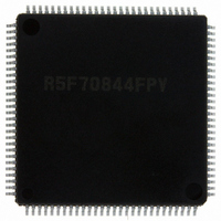
DF70844AD80FPV Renesas Electronics America, DF70844AD80FPV Datasheet - Page 394

DF70844AD80FPV
Manufacturer Part Number
DF70844AD80FPV
Description
IC SUPERH MCU FLASH 112LQFP
Manufacturer
Renesas Electronics America
Series
SuperH® SH7080r
Datasheet
1.DF70844AD80FPV.pdf
(1644 pages)
Specifications of DF70844AD80FPV
Core Size
32-Bit
Program Memory Size
256KB (256K x 8)
Core Processor
SH-2
Speed
80MHz
Connectivity
EBI/EMI, FIFO, I²C, SCI, SSU
Peripherals
DMA, POR, PWM, WDT
Number Of I /o
76
Program Memory Type
FLASH
Ram Size
16K x 8
Voltage - Supply (vcc/vdd)
3 V ~ 5.5 V
Data Converters
A/D 8x10b
Oscillator Type
Internal
Operating Temperature
-40°C ~ 85°C
Package / Case
112-LQFP
No. Of I/o's
76
Ram Memory Size
16KB
Cpu Speed
80MHz
Digital Ic Case Style
LQFP
Supply Voltage Range
3V To 3.6V, 4.5V To 5.5V
Embedded Interface Type
I2C, SCI
Rohs Compliant
Yes
Lead Free Status / RoHS Status
Lead free / RoHS Compliant
For Use With
R0K570865S001BE - KIT STARTER FOR SH7086R0K570865S000BE - KIT STARTER FOR SH7086HS0005KCU11H - EMULATOR E10A-USB H8S(X),SH2(A)
Eeprom Size
-
Lead Free Status / RoHS Status
Lead free / RoHS Compliant, Lead free / RoHS Compliant
Available stocks
Company
Part Number
Manufacturer
Quantity
Price
Company:
Part Number:
DF70844AD80FPV
Manufacturer:
Renesas Electronics America
Quantity:
10 000
- Current page: 394 of 1644
- Download datasheet (10Mb)
Section 9 Bus State Controller (BSC)
Mode register setting timing is shown in figure 9.30. A PALL command (all bank precharge
command) is firstly issued. An REF command (auto-refresh command) is then issued 8 times. An
MRS command (mode register write command) is finally issued. Idle cycles, of which number is
specified by the WTRP[1:0] bits in CS3WCR, are inserted between the PALL and the first REF.
Idle cycles, of which number is specified by the WTRC[1:0] bits in CS3WCR, are inserted
between REF and REF, and between the 8th REF and MRS. Idle cycles, of which number is one
or more, are inserted between the MRS and a command to be issued next.
It is necessary to keep idle time of certain cycles for SDRAM after power-on before issuing PALL
command. Refer to the manual of the SDRAM for the idle time to be needed. When the pulse
width of the reset signal is longer than the idle time, mode register setting can be started
immediately after the reset, but care should be taken when the pulse width of the reset signal is
shorter than the idle time.
Rev. 3.00 May 17, 2007 Page 336 of 1582
REJ09B0181-0300
RASL, RASU
CASL, CASU
A12/A11*
D31 to D0
A25 to A0
DACKn*
Notes:
DQMxx
RDWR
CSn
CK
BS
1
2
1.
2.
Figure 9.30 SDRAM Mode Register Write Timing (Based on JEDEC)
Address pin to be connected to pin A10 of SDRAM.
The waveform for DACKn is when active low is specified.
PALL
Tp
Tpw
REF
Trr
Trc
Trc
REF
Hi-Z
Trr
Trc
Trc
MRS
Tmw
Tnop
Related parts for DF70844AD80FPV
Image
Part Number
Description
Manufacturer
Datasheet
Request
R

Part Number:
Description:
KIT STARTER FOR M16C/29
Manufacturer:
Renesas Electronics America
Datasheet:

Part Number:
Description:
KIT STARTER FOR R8C/2D
Manufacturer:
Renesas Electronics America
Datasheet:

Part Number:
Description:
R0K33062P STARTER KIT
Manufacturer:
Renesas Electronics America
Datasheet:

Part Number:
Description:
KIT STARTER FOR R8C/23 E8A
Manufacturer:
Renesas Electronics America
Datasheet:

Part Number:
Description:
KIT STARTER FOR R8C/25
Manufacturer:
Renesas Electronics America
Datasheet:

Part Number:
Description:
KIT STARTER H8S2456 SHARPE DSPLY
Manufacturer:
Renesas Electronics America
Datasheet:

Part Number:
Description:
KIT STARTER FOR R8C38C
Manufacturer:
Renesas Electronics America
Datasheet:

Part Number:
Description:
KIT STARTER FOR R8C35C
Manufacturer:
Renesas Electronics America
Datasheet:

Part Number:
Description:
KIT STARTER FOR R8CL3AC+LCD APPS
Manufacturer:
Renesas Electronics America
Datasheet:

Part Number:
Description:
KIT STARTER FOR RX610
Manufacturer:
Renesas Electronics America
Datasheet:

Part Number:
Description:
KIT STARTER FOR R32C/118
Manufacturer:
Renesas Electronics America
Datasheet:

Part Number:
Description:
KIT DEV RSK-R8C/26-29
Manufacturer:
Renesas Electronics America
Datasheet:

Part Number:
Description:
KIT STARTER FOR SH7124
Manufacturer:
Renesas Electronics America
Datasheet:

Part Number:
Description:
KIT STARTER FOR H8SX/1622
Manufacturer:
Renesas Electronics America
Datasheet:

Part Number:
Description:
KIT DEV FOR SH7203
Manufacturer:
Renesas Electronics America
Datasheet:


