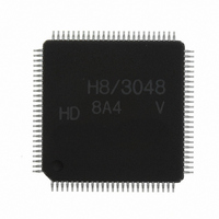
HD64F3048VTF8 Renesas Electronics America, HD64F3048VTF8 Datasheet - Page 162

HD64F3048VTF8
Manufacturer Part Number
HD64F3048VTF8
Description
IC H8 MCU FLASH 128K 100-QFP
Manufacturer
Renesas Electronics America
Series
H8® H8/300Hr
Datasheet
1.HD64F3048F16.pdf
(907 pages)
Specifications of HD64F3048VTF8
Core Processor
H8/300H
Core Size
16-Bit
Speed
8MHz
Connectivity
SCI, SmartCard
Peripherals
DMA, PWM, WDT
Number Of I /o
70
Program Memory Size
128KB (128K x 8)
Program Memory Type
FLASH
Ram Size
4K x 8
Voltage - Supply (vcc/vdd)
2.7 V ~ 5.5 V
Data Converters
A/D 8x10b; D/A 2x8b
Oscillator Type
Internal
Operating Temperature
-20°C ~ 75°C
Package / Case
100-TQFP, 100-VQFP
Lead Free Status / RoHS Status
Contains lead / RoHS non-compliant
Eeprom Size
-
Other names
HD64F3048VX8
- Current page: 162 of 907
- Download datasheet (6Mb)
Section 6 Bus Controller
6.3.3
The H8/3048 Group allows either 8-bit access or 16-bit access to be designated for each of areas
7 to 0. An 8-bit-access area uses the upper data bus (D
upper data bus (D
In read access the RD signal applies without distinction to both the upper and lower data bus. In
write access the HWR signal applies to the upper data bus, and the LWR signal applies to the
lower data bus.
Table 6.4 indicates how the two parts of the data bus are used under different access conditions.
Table 6.4
Area
8-bit-access
area
16-bit-access
area
Note: Undetermined data means that unpredictable data is output.
Rev. 7.00 Sep 21, 2005 page 136 of 878
REJ09B0259-0700
Invalid means that the bus is in the input state and the input is ignored.
Data Bus
Access Conditions and Data Bus Usage
Access
Size
—
Byte
Word
15
to D
8
) and lower data bus (D
Read/W
rite
Read
Write
Read
Write
Read
Write
Address
—
—
Even
Odd
Even
Odd
—
—
Valid
Strobe
RD
HWR
RD
HWR
LWR
RD
HWR,
LWR
7
to D
15
0
).
to D
Upper Data Bus
(D
Valid
Valid
Invalid
Valid
Undetermined data
Valid
Valid
15
8
to D
). A 16-bit-access area uses both the
8
)
Valid
Valid
Lower Data Bus
(D
Invalid
Undetermined data
Invalid
Undetermined data
Valid
Valid
7
to D
0
)
Related parts for HD64F3048VTF8
Image
Part Number
Description
Manufacturer
Datasheet
Request
R

Part Number:
Description:
KIT STARTER FOR M16C/29
Manufacturer:
Renesas Electronics America
Datasheet:

Part Number:
Description:
KIT STARTER FOR R8C/2D
Manufacturer:
Renesas Electronics America
Datasheet:

Part Number:
Description:
R0K33062P STARTER KIT
Manufacturer:
Renesas Electronics America
Datasheet:

Part Number:
Description:
KIT STARTER FOR R8C/23 E8A
Manufacturer:
Renesas Electronics America
Datasheet:

Part Number:
Description:
KIT STARTER FOR R8C/25
Manufacturer:
Renesas Electronics America
Datasheet:

Part Number:
Description:
KIT STARTER H8S2456 SHARPE DSPLY
Manufacturer:
Renesas Electronics America
Datasheet:

Part Number:
Description:
KIT STARTER FOR R8C38C
Manufacturer:
Renesas Electronics America
Datasheet:

Part Number:
Description:
KIT STARTER FOR R8C35C
Manufacturer:
Renesas Electronics America
Datasheet:

Part Number:
Description:
KIT STARTER FOR R8CL3AC+LCD APPS
Manufacturer:
Renesas Electronics America
Datasheet:

Part Number:
Description:
KIT STARTER FOR RX610
Manufacturer:
Renesas Electronics America
Datasheet:

Part Number:
Description:
KIT STARTER FOR R32C/118
Manufacturer:
Renesas Electronics America
Datasheet:

Part Number:
Description:
KIT DEV RSK-R8C/26-29
Manufacturer:
Renesas Electronics America
Datasheet:

Part Number:
Description:
KIT STARTER FOR SH7124
Manufacturer:
Renesas Electronics America
Datasheet:

Part Number:
Description:
KIT STARTER FOR H8SX/1622
Manufacturer:
Renesas Electronics America
Datasheet:


