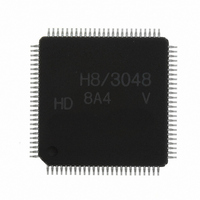
HD64F3048VTF8 Renesas Electronics America, HD64F3048VTF8 Datasheet - Page 554

HD64F3048VTF8
Manufacturer Part Number
HD64F3048VTF8
Description
IC H8 MCU FLASH 128K 100-QFP
Manufacturer
Renesas Electronics America
Series
H8® H8/300Hr
Datasheet
1.HD64F3048F16.pdf
(907 pages)
Specifications of HD64F3048VTF8
Core Processor
H8/300H
Core Size
16-Bit
Speed
8MHz
Connectivity
SCI, SmartCard
Peripherals
DMA, PWM, WDT
Number Of I /o
70
Program Memory Size
128KB (128K x 8)
Program Memory Type
FLASH
Ram Size
4K x 8
Voltage - Supply (vcc/vdd)
2.7 V ~ 5.5 V
Data Converters
A/D 8x10b; D/A 2x8b
Oscillator Type
Internal
Operating Temperature
-20°C ~ 75°C
Package / Case
100-TQFP, 100-VQFP
Lead Free Status / RoHS Status
Contains lead / RoHS non-compliant
Eeprom Size
-
Other names
HD64F3048VX8
- Current page: 554 of 907
- Download datasheet (6Mb)
Section 14 Smart Card Interface
This procedure may include interrupt handling and DMA transfer.
If the RIE bit is set to 1 to enable interrupt requests, when receiving is completed and the RDRF
flag is set to 1, a receive-data-full interrupt (RXI) is requested. If a receive error occurs, either the
ORER or PER flag is set to 1 and a transmit/receive-error interrupt (ERI) is requested.
If the RXI interrupt activates the DMAC, the number of bytes designated in the DMAC will be
transferred, skipping receive data in which an error occurred.
For details, see Interrupt Operations and Data Transfer by DMAC below.
When a parity error occurs and PER is set to 1, the receive data is transferred to RDR, so the
erroneous data can be read.
Switching Modes: To switch from receive mode to transmit mode, check that receiving
operations have completed, then initialize the smart card interface, clearing RE to 0 and setting TE
to 1. Completion of receive operations is indicated by the RDRF, PER, or ORER flag.
To switch from transmit mode to receive mode, check that transmitting operations have
completed, then initialize the smart card interface, clearing TE to 0 and setting RE to 1.
Completion of transmit operations can be verified from the TEND flag.
Fixing Clock Output: When the GM bit of the SMR is set to 1, clock output is fixed by CKE1
and CKE0 of SCR. In this case, the clock pulse can be set at minimum value.
Figure 14.8 shows clock output fixed timing: CKE0 is restricted with GM = 1 and CKE1 = 1.
SCK
Rev. 7.00 Sep 21, 2005 page 528 of 878
REJ09B0259-0700
Specified pulse width
SCR write
(CKE0 = 0)
Figure 14.8 Clock Output Fixed Timing
CKE1 value
SCR write
(CKE0 = 1)
Specified pulse width
Related parts for HD64F3048VTF8
Image
Part Number
Description
Manufacturer
Datasheet
Request
R

Part Number:
Description:
KIT STARTER FOR M16C/29
Manufacturer:
Renesas Electronics America
Datasheet:

Part Number:
Description:
KIT STARTER FOR R8C/2D
Manufacturer:
Renesas Electronics America
Datasheet:

Part Number:
Description:
R0K33062P STARTER KIT
Manufacturer:
Renesas Electronics America
Datasheet:

Part Number:
Description:
KIT STARTER FOR R8C/23 E8A
Manufacturer:
Renesas Electronics America
Datasheet:

Part Number:
Description:
KIT STARTER FOR R8C/25
Manufacturer:
Renesas Electronics America
Datasheet:

Part Number:
Description:
KIT STARTER H8S2456 SHARPE DSPLY
Manufacturer:
Renesas Electronics America
Datasheet:

Part Number:
Description:
KIT STARTER FOR R8C38C
Manufacturer:
Renesas Electronics America
Datasheet:

Part Number:
Description:
KIT STARTER FOR R8C35C
Manufacturer:
Renesas Electronics America
Datasheet:

Part Number:
Description:
KIT STARTER FOR R8CL3AC+LCD APPS
Manufacturer:
Renesas Electronics America
Datasheet:

Part Number:
Description:
KIT STARTER FOR RX610
Manufacturer:
Renesas Electronics America
Datasheet:

Part Number:
Description:
KIT STARTER FOR R32C/118
Manufacturer:
Renesas Electronics America
Datasheet:

Part Number:
Description:
KIT DEV RSK-R8C/26-29
Manufacturer:
Renesas Electronics America
Datasheet:

Part Number:
Description:
KIT STARTER FOR SH7124
Manufacturer:
Renesas Electronics America
Datasheet:

Part Number:
Description:
KIT STARTER FOR H8SX/1622
Manufacturer:
Renesas Electronics America
Datasheet:


