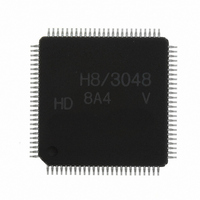
HD64F3048VTF8 Renesas Electronics America, HD64F3048VTF8 Datasheet - Page 173

HD64F3048VTF8
Manufacturer Part Number
HD64F3048VTF8
Description
IC H8 MCU FLASH 128K 100-QFP
Manufacturer
Renesas Electronics America
Series
H8® H8/300Hr
Datasheet
1.HD64F3048F16.pdf
(907 pages)
Specifications of HD64F3048VTF8
Core Processor
H8/300H
Core Size
16-Bit
Speed
8MHz
Connectivity
SCI, SmartCard
Peripherals
DMA, PWM, WDT
Number Of I /o
70
Program Memory Size
128KB (128K x 8)
Program Memory Type
FLASH
Ram Size
4K x 8
Voltage - Supply (vcc/vdd)
2.7 V ~ 5.5 V
Data Converters
A/D 8x10b; D/A 2x8b
Oscillator Type
Internal
Operating Temperature
-20°C ~ 75°C
Package / Case
100-TQFP, 100-VQFP
Lead Free Status / RoHS Status
Contains lead / RoHS non-compliant
Eeprom Size
-
Other names
HD64F3048VX8
- Current page: 173 of 907
- Download datasheet (6Mb)
Wait Modes in Areas Where Wait-State Controller is Enabled
External three-state access areas in which the wait-state controller is enabled (ASTn = 1, WCEn =
1) can operate in pin wait mode 1, pin auto-wait mode, or programmable wait mode, as selected by
bits WMS1 and WMS0. Bits WMS1 and WMS0 apply to all areas, so all areas in which the wait-
state controller is enabled operate in the same wait mode.
Pin Wait Mode 1: In all accesses to external three-state-access areas, the number of wait states
(T
clock ( ) in the last of these wait states, an additional wait state is inserted. If the WAIT pin
remains low, wait states continue to be inserted until the WAIT signal goes high.
Pin wait mode 1 is useful for inserting four or more wait states, or for inserting different numbers
of wait states for different external devices.
If the wait count is 0, this mode operates in the same way as pin wait mode 0.
Figure 6.13 shows the timing when the wait count is 1 (WC1 = 0, WC0 = 1) and one additional
wait state is inserted by WAIT input.
W
) selected by bits WC1 and WC0 are inserted. If the WAIT pin is low at the fall of the system
Read
access
Write
access
Note:
*
Arrows indicate time of sampling of the
WAIT
Address bus
AS
RD
Data bus
HWR, LWR
Data bus
pin
Figure 6.13 Pin Wait Mode 1
T
1
T
WAIT
2
pin.
External address
Inserted by
wait count
Write data
Write data
T
Rev. 7.00 Sep 21, 2005 page 147 of 878
W
*
Inserted by
WAIT
T
W
signal
*
Section 6 Bus Controller
Read data
T
3
REJ09B0259-0700
Related parts for HD64F3048VTF8
Image
Part Number
Description
Manufacturer
Datasheet
Request
R

Part Number:
Description:
KIT STARTER FOR M16C/29
Manufacturer:
Renesas Electronics America
Datasheet:

Part Number:
Description:
KIT STARTER FOR R8C/2D
Manufacturer:
Renesas Electronics America
Datasheet:

Part Number:
Description:
R0K33062P STARTER KIT
Manufacturer:
Renesas Electronics America
Datasheet:

Part Number:
Description:
KIT STARTER FOR R8C/23 E8A
Manufacturer:
Renesas Electronics America
Datasheet:

Part Number:
Description:
KIT STARTER FOR R8C/25
Manufacturer:
Renesas Electronics America
Datasheet:

Part Number:
Description:
KIT STARTER H8S2456 SHARPE DSPLY
Manufacturer:
Renesas Electronics America
Datasheet:

Part Number:
Description:
KIT STARTER FOR R8C38C
Manufacturer:
Renesas Electronics America
Datasheet:

Part Number:
Description:
KIT STARTER FOR R8C35C
Manufacturer:
Renesas Electronics America
Datasheet:

Part Number:
Description:
KIT STARTER FOR R8CL3AC+LCD APPS
Manufacturer:
Renesas Electronics America
Datasheet:

Part Number:
Description:
KIT STARTER FOR RX610
Manufacturer:
Renesas Electronics America
Datasheet:

Part Number:
Description:
KIT STARTER FOR R32C/118
Manufacturer:
Renesas Electronics America
Datasheet:

Part Number:
Description:
KIT DEV RSK-R8C/26-29
Manufacturer:
Renesas Electronics America
Datasheet:

Part Number:
Description:
KIT STARTER FOR SH7124
Manufacturer:
Renesas Electronics America
Datasheet:

Part Number:
Description:
KIT STARTER FOR H8SX/1622
Manufacturer:
Renesas Electronics America
Datasheet:


