HD64F3048VTF8 Renesas Electronics America, HD64F3048VTF8 Datasheet - Page 43
HD64F3048VTF8
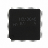
Manufacturer Part Number
HD64F3048VTF8
Description
IC H8 MCU FLASH 128K 100-QFP
Manufacturer
Renesas Electronics America
Series
H8® H8/300Hr
Datasheet
1.HD64F3048F16.pdf
(907 pages)
Specifications of HD64F3048VTF8
Core Processor
H8/300H
Core Size
16-Bit
Speed
8MHz
Connectivity
SCI, SmartCard
Peripherals
DMA, PWM, WDT
Number Of I /o
70
Program Memory Size
128KB (128K x 8)
Program Memory Type
FLASH
Ram Size
4K x 8
Voltage - Supply (vcc/vdd)
2.7 V ~ 5.5 V
Data Converters
A/D 8x10b; D/A 2x8b
Oscillator Type
Internal
Operating Temperature
-20°C ~ 75°C
Package / Case
100-TQFP, 100-VQFP
Lead Free Status / RoHS Status
Contains lead / RoHS non-compliant
Eeprom Size
-
Other names
HD64F3048VX8


Type
Refresh
controller
DMA controller
(DMAC)
16-bit integrated
timer unit (ITU)
Symbol
RFSH
CS
RD
HWR
LWR
DREQ
DREQ
TEND
TEND
TCLKD to
TCLKA
TIOCA
TIOCA
TIOCB
TIOCB
TOCXA
TOCXB
3
1
0
1
0
4
0
4
0
,
,
4
4
to
to
Pin No.
87
88
70
71
72
9, 8
94, 93
96 to 93
4, 2, 99,
97, 95
5, 3, 100,
98, 96
6
7
I/O
Output
Output
Output
Output
Output
Input
Output
Input
Input/
output
Input/
output
Output
Output
Name and Function
Refresh: Indicates a refresh cycle
Row address strobe RAS
strobe signal for DRAM connected to area 3
Column address strobe CAS
address strobe signal for DRAM connected
to area 3; used with 2WE DRAM.
Write enable WE
DRAM connected to area 3; used with
2CAS DRAM.
Upper write UW
DRAM connected to area 3; used with 2WE
DRAM.
Upper column address strobe UCAS
Column address strobe signal for DRAM
connected to area 3; used with 2CAS
DRAM.
Lower write LW
DRAM connected to area 3; used with 2WE
DRAM.
Lower column address strobe LCAS
Column address strobe signal for DRAM
connected to area 3; used with 2CAS
DRAM.
DMA request 1 and 0: DMAC activation
requests
Transfer end 1 and 0: These signals
indicate that the DMAC has ended a data
transfer
Clock input D to A: External clock inputs
Input capture/output compare A4 to A0:
GRA4 to GRA0 output compare or input
capture, or PWM output
Input capture/output compare B4 to B0:
GRB4 to GRB0 output compare or input
capture
Output compare XA4: PWM output
Output compare XB4: PWM output
Rev. 7.00 Sep 21, 2005 page 17 of 878
UW: Write enable signal for
UW
UW
LW: Write enable signal for
LW
LW
WE
WE
WE: Write enable signal for
RAS: Row address
RAS
RAS
Section 1 Overview
REJ09B0259-0700
CAS: Column
CAS
CAS
UCAS:
UCAS
UCAS
LCAS
LCAS:
LCAS
Related parts for HD64F3048VTF8
Image
Part Number
Description
Manufacturer
Datasheet
Request
R


Part Number:
Description:
KIT STARTER FOR M16C/29
Manufacturer:
Renesas Electronics America
Datasheet:

Part Number:
Description:
KIT STARTER FOR R8C/2D
Manufacturer:
Renesas Electronics America
Datasheet:

Part Number:
Description:
R0K33062P STARTER KIT
Manufacturer:
Renesas Electronics America
Datasheet:

Part Number:
Description:
KIT STARTER FOR R8C/23 E8A
Manufacturer:
Renesas Electronics America
Datasheet:

Part Number:
Description:
KIT STARTER FOR R8C/25
Manufacturer:
Renesas Electronics America
Datasheet:

Part Number:
Description:
KIT STARTER H8S2456 SHARPE DSPLY
Manufacturer:
Renesas Electronics America
Datasheet:

Part Number:
Description:
KIT STARTER FOR R8C38C
Manufacturer:
Renesas Electronics America
Datasheet:

Part Number:
Description:
KIT STARTER FOR R8C35C
Manufacturer:
Renesas Electronics America
Datasheet:

Part Number:
Description:
KIT STARTER FOR R8CL3AC+LCD APPS
Manufacturer:
Renesas Electronics America
Datasheet:
Part Number:
Description:
KIT STARTER FOR RX610
Manufacturer:
Renesas Electronics America
Datasheet:

Part Number:
Description:
KIT STARTER FOR R32C/118
Manufacturer:
Renesas Electronics America
Datasheet:

Part Number:
Description:
KIT DEV RSK-R8C/26-29
Manufacturer:
Renesas Electronics America
Datasheet:

Part Number:
Description:
KIT STARTER FOR SH7124
Manufacturer:
Renesas Electronics America
Datasheet:

Part Number:
Description:
KIT STARTER FOR H8SX/1622
Manufacturer:
Renesas Electronics America
Datasheet: