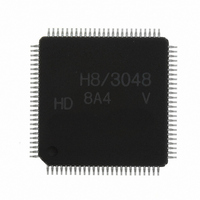
HD64F3048VTF8 Renesas Electronics America, HD64F3048VTF8 Datasheet - Page 96

HD64F3048VTF8
Manufacturer Part Number
HD64F3048VTF8
Description
IC H8 MCU FLASH 128K 100-QFP
Manufacturer
Renesas Electronics America
Series
H8® H8/300Hr
Datasheet
1.HD64F3048F16.pdf
(907 pages)
Specifications of HD64F3048VTF8
Core Processor
H8/300H
Core Size
16-Bit
Speed
8MHz
Connectivity
SCI, SmartCard
Peripherals
DMA, PWM, WDT
Number Of I /o
70
Program Memory Size
128KB (128K x 8)
Program Memory Type
FLASH
Ram Size
4K x 8
Voltage - Supply (vcc/vdd)
2.7 V ~ 5.5 V
Data Converters
A/D 8x10b; D/A 2x8b
Oscillator Type
Internal
Operating Temperature
-20°C ~ 75°C
Package / Case
100-TQFP, 100-VQFP
Lead Free Status / RoHS Status
Contains lead / RoHS non-compliant
Eeprom Size
-
Other names
HD64F3048VX8
- Current page: 96 of 907
- Download datasheet (6Mb)
Section 3 MCU Operating Modes
3.4.6
Ports 1, 2, and 5 and part of port A function as address pins A
maximum 16-Mbyte address space, but following a reset they are input ports. To use ports 1, 2,
and 5 as an address bus, the corresponding bits in their data direction registers (P1DDR, P2DDR,
and P5DDR) must be set to 1. For A
A
The initial bus mode after a reset is 8 bits, with 8-bit access to all areas. If at least one area is
designated for 16-bit access in ABWCR, the bus mode switches to 16 bits.
3.4.7
This mode operates using the on-chip ROM, RAM, and internal I/O registers. All I/O ports are
available. Mode 7 supports a 1-Mbyte address space.
3.5
The pin functions of ports 1 to 5 and port A vary depending on the operating mode. Table 3.3
indicates their functions in each operating mode.
Table 3.3
Port
Port 1
Port 2
Port 3
Port 4
Port 5
Port A
Notes: 1. Initial state. The bus mode can be switched by settings in ABWCR. These pins function
Rev. 7.00 Sep 21, 2005 page 70 of 878
REJ09B0259-0700
20
is always used for address output.)
2. Initial state. These pins become address output pins when the corresponding bits in the
3. Initial state. A
Mode 1
A
A
D
P4
A
PA
Mode 6
Mode 7
Pin Functions in Each Operating Mode
7
15
19
15
7
as P4
data direction registers (P1DDR, P2DDR, P5DDR) are set to 1.
A
to A
7
to A
to A
to D
to P4
to PA
21
Pin Functions in Each Mode
0
output by writing 0 in bits 7 to 5 of BRCR.
8
16
8
7
0
4
*
to P4
1
Mode 2
A
A
D
D
A
PA
7
15
19
15
7
0
to A
to D
7
20
to A
to D
to A
in 8-bit bus mode, and as D
to PA
is always an address output pin. PA
0
0
8
16
8
*
1
4
Mode 3
A
A
D
P4
A
PA
A
7
15
19
20
23
15
7
to A
7
to A
to D
to A
to A
to P4
to PA
0
8
16
8
21
0
5
*
*
1
output, clear bits 7 to 5 of BRCR to 0. (In this mode
3
,
Mode 4
A
A
D
D
A
PA
A
7
15
19
20
15
7
to A
to D
7
to A
to D
to A
to PA
7
0
0
to D
8
16
8
*
1
5
*
3
0
,
in 16-bit bus mode.
Mode 5
P1
P2
D
P4
P5
PA
23
15
7
7
7
7
3
7
to A
to D
to PA
to P1
to P2
to P4
to P5
to PA
8
0
, permitting access to a
0
0
0
0
4
5
*
*
*
*
2
2
1
2
are switched over to A
Mode 6
P1
P2
D
P4
P5
PA
A
20
15
7
7
7
3
7
*
to D
to P1
to P2
to P4
to P5
3
to PA
8
0
0
0
0
5
*
*
*
*
,
2
2
1
2
Mode 7
P1
P2
P3
P4
P5
PA
7
7
7
7
3
7
to P1
to P2
to P3
to P4
to P5
to PA
23
0
0
0
0
0
4
to
Related parts for HD64F3048VTF8
Image
Part Number
Description
Manufacturer
Datasheet
Request
R

Part Number:
Description:
KIT STARTER FOR M16C/29
Manufacturer:
Renesas Electronics America
Datasheet:

Part Number:
Description:
KIT STARTER FOR R8C/2D
Manufacturer:
Renesas Electronics America
Datasheet:

Part Number:
Description:
R0K33062P STARTER KIT
Manufacturer:
Renesas Electronics America
Datasheet:

Part Number:
Description:
KIT STARTER FOR R8C/23 E8A
Manufacturer:
Renesas Electronics America
Datasheet:

Part Number:
Description:
KIT STARTER FOR R8C/25
Manufacturer:
Renesas Electronics America
Datasheet:

Part Number:
Description:
KIT STARTER H8S2456 SHARPE DSPLY
Manufacturer:
Renesas Electronics America
Datasheet:

Part Number:
Description:
KIT STARTER FOR R8C38C
Manufacturer:
Renesas Electronics America
Datasheet:

Part Number:
Description:
KIT STARTER FOR R8C35C
Manufacturer:
Renesas Electronics America
Datasheet:

Part Number:
Description:
KIT STARTER FOR R8CL3AC+LCD APPS
Manufacturer:
Renesas Electronics America
Datasheet:

Part Number:
Description:
KIT STARTER FOR RX610
Manufacturer:
Renesas Electronics America
Datasheet:

Part Number:
Description:
KIT STARTER FOR R32C/118
Manufacturer:
Renesas Electronics America
Datasheet:

Part Number:
Description:
KIT DEV RSK-R8C/26-29
Manufacturer:
Renesas Electronics America
Datasheet:

Part Number:
Description:
KIT STARTER FOR SH7124
Manufacturer:
Renesas Electronics America
Datasheet:

Part Number:
Description:
KIT STARTER FOR H8SX/1622
Manufacturer:
Renesas Electronics America
Datasheet:


