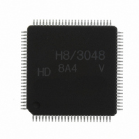
HD64F3048VTF8 Renesas Electronics America, HD64F3048VTF8 Datasheet - Page 631

HD64F3048VTF8
Manufacturer Part Number
HD64F3048VTF8
Description
IC H8 MCU FLASH 128K 100-QFP
Manufacturer
Renesas Electronics America
Series
H8® H8/300Hr
Datasheet
1.HD64F3048F16.pdf
(907 pages)
Specifications of HD64F3048VTF8
Core Processor
H8/300H
Core Size
16-Bit
Speed
8MHz
Connectivity
SCI, SmartCard
Peripherals
DMA, PWM, WDT
Number Of I /o
70
Program Memory Size
128KB (128K x 8)
Program Memory Type
FLASH
Ram Size
4K x 8
Voltage - Supply (vcc/vdd)
2.7 V ~ 5.5 V
Data Converters
A/D 8x10b; D/A 2x8b
Oscillator Type
Internal
Operating Temperature
-20°C ~ 75°C
Package / Case
100-TQFP, 100-VQFP
Lead Free Status / RoHS Status
Contains lead / RoHS non-compliant
Eeprom Size
-
Other names
HD64F3048VX8
- Current page: 631 of 907
- Download datasheet (6Mb)
19.5.1
To write data into the flash memory, follow the programming algorithm shown in figure 19.9.
This programming algorithm can write data without subjecting the device to voltage stress or
impairing the reliability of programmed data.
To program data, first set the V
programmed by erase block registers 1 and 2 (EBR1, EBR2), and write the data to the address to
be programmed, as in writing to RAM. The flash memory latches the address and data in an
address latch and data latch. Next set the P bit in FLMCR, selecting program mode. The
programming duration is the time during which the P bit is set. A software timer should be used to
provide an initial programming duration of 15.8 µs or less. Programming for too long a time, due
to program runaway for example, can cause device damage. Before selecting program mode, set
up the watchdog timer so as to prevent overprogramming.
19.5.2
In program-verify mode, after data has been programmed in program mode, the data is read to
check that it has been programmed correctly.
After the programming time has elapsed, exit programming mode (clear the P bit to 0) and select
program-verify mode (set the PV bit to 1). In program-verify mode, a program-verify voltage is
applied to the memory cells at the latched address. If the flash memory is read in this state, the
data at the latched address will be read. After selecting program-verify mode, wait 4 µs before
reading, then compare the programmed data with the verify data. If they agree, exit program-
verify mode and program the next address. If they do not agree, select program mode again and
repeat the same program and program-verify sequence. Do not repeat the program and program-
verify sequence more than 6 times for the same bit. (When a bit is programmed repeatedly, set a
loop counter so that the total programming time will not exceed 1 ms.)
Program Mode
Program-Verify Mode
Section 19 Flash Memory (H8/3048F: Dual Power Supply (V
PP
E bit in FLMCR, wait 5 to 10 µs, then designate the blocks to be
Rev. 7.00 Sep 21, 2005 page 605 of 878
REJ09B0259-0700
PP
= 12 V))
Related parts for HD64F3048VTF8
Image
Part Number
Description
Manufacturer
Datasheet
Request
R

Part Number:
Description:
KIT STARTER FOR M16C/29
Manufacturer:
Renesas Electronics America
Datasheet:

Part Number:
Description:
KIT STARTER FOR R8C/2D
Manufacturer:
Renesas Electronics America
Datasheet:

Part Number:
Description:
R0K33062P STARTER KIT
Manufacturer:
Renesas Electronics America
Datasheet:

Part Number:
Description:
KIT STARTER FOR R8C/23 E8A
Manufacturer:
Renesas Electronics America
Datasheet:

Part Number:
Description:
KIT STARTER FOR R8C/25
Manufacturer:
Renesas Electronics America
Datasheet:

Part Number:
Description:
KIT STARTER H8S2456 SHARPE DSPLY
Manufacturer:
Renesas Electronics America
Datasheet:

Part Number:
Description:
KIT STARTER FOR R8C38C
Manufacturer:
Renesas Electronics America
Datasheet:

Part Number:
Description:
KIT STARTER FOR R8C35C
Manufacturer:
Renesas Electronics America
Datasheet:

Part Number:
Description:
KIT STARTER FOR R8CL3AC+LCD APPS
Manufacturer:
Renesas Electronics America
Datasheet:

Part Number:
Description:
KIT STARTER FOR RX610
Manufacturer:
Renesas Electronics America
Datasheet:

Part Number:
Description:
KIT STARTER FOR R32C/118
Manufacturer:
Renesas Electronics America
Datasheet:

Part Number:
Description:
KIT DEV RSK-R8C/26-29
Manufacturer:
Renesas Electronics America
Datasheet:

Part Number:
Description:
KIT STARTER FOR SH7124
Manufacturer:
Renesas Electronics America
Datasheet:

Part Number:
Description:
KIT STARTER FOR H8SX/1622
Manufacturer:
Renesas Electronics America
Datasheet:


