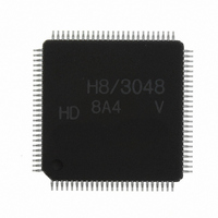
HD64F3048VTF8 Renesas Electronics America, HD64F3048VTF8 Datasheet - Page 520

HD64F3048VTF8
Manufacturer Part Number
HD64F3048VTF8
Description
IC H8 MCU FLASH 128K 100-QFP
Manufacturer
Renesas Electronics America
Series
H8® H8/300Hr
Datasheet
1.HD64F3048F16.pdf
(907 pages)
Specifications of HD64F3048VTF8
Core Processor
H8/300H
Core Size
16-Bit
Speed
8MHz
Connectivity
SCI, SmartCard
Peripherals
DMA, PWM, WDT
Number Of I /o
70
Program Memory Size
128KB (128K x 8)
Program Memory Type
FLASH
Ram Size
4K x 8
Voltage - Supply (vcc/vdd)
2.7 V ~ 5.5 V
Data Converters
A/D 8x10b; D/A 2x8b
Oscillator Type
Internal
Operating Temperature
-20°C ~ 75°C
Package / Case
100-TQFP, 100-VQFP
Lead Free Status / RoHS Status
Contains lead / RoHS non-compliant
Eeprom Size
-
Other names
HD64F3048VX8
- Current page: 520 of 907
- Download datasheet (6Mb)
Section 13 Serial Communication Interface
13.3.4
In synchronous mode, the SCI transmits and receives data in synchronization with clock pulses.
This mode is suitable for high-speed serial communication.
The SCI transmitter and receiver share the same clock but are otherwise independent, so full
duplex communication is possible. The transmitter and receiver are also double buffered, so
continuous transmitting or receiving is possible by reading or writing data while transmitting or
receiving is in progress.
Figure 13.14 shows the general format in synchronous serial communication.
In synchronous serial communication, each data bit is placed on the communication line from one
falling edge of the serial clock to the next. Data is guaranteed valid at the rise of the serial clock.
In each character, the serial data bits are transmitted in order from LSB (first) to MSB (last). After
output of the MSB, the communication line remains in the state of the MSB. In synchronous mode
the SCI receives data by synchronizing with the rise of the serial clock.
Communication Format: The data length is fixed at 8 bits. No parity bit or multiprocessor bit
can be added.
Clock: An internal clock generated by the on-chip baud rate generator or an external clock input
from the SCK pin can be selected by clearing or setting the CKE1 bit in SCR. See table 13.9.
When the SCI operates on an internal clock, it outputs the clock signal at the SCK pin. Eight clock
pulses are output per transmitted or received character.
When the SCI operates on an internal clock, the serial clock outputs the clock signal at the SCK
pin. Eight clock pulses are output per transmitted or received character. When the SCI is not
transmitting or receiving, the clock signal remains in the high state. However, when receiving
only, overrun error may occur or the serial clock continues output until the RE bit clears at 0.
When transmitting or receiving in single characters, select the external clock.
Rev. 7.00 Sep 21, 2005 page 494 of 878
REJ09B0259-0700
Synchronous Operation
Serial data
Serial clock
Note:
*
High except in continuous transmitting or receiving
Figure 13.14 Data Format in Synchronous Communication
Don’t care
*
Bit 0
LSB
Bit 1
One unit (character or frame) of serial data
Bit 2
Bit 3
Bit 4
Bit 5
Bit 6
Bit 7
MSB
Don’t care
*
Related parts for HD64F3048VTF8
Image
Part Number
Description
Manufacturer
Datasheet
Request
R

Part Number:
Description:
KIT STARTER FOR M16C/29
Manufacturer:
Renesas Electronics America
Datasheet:

Part Number:
Description:
KIT STARTER FOR R8C/2D
Manufacturer:
Renesas Electronics America
Datasheet:

Part Number:
Description:
R0K33062P STARTER KIT
Manufacturer:
Renesas Electronics America
Datasheet:

Part Number:
Description:
KIT STARTER FOR R8C/23 E8A
Manufacturer:
Renesas Electronics America
Datasheet:

Part Number:
Description:
KIT STARTER FOR R8C/25
Manufacturer:
Renesas Electronics America
Datasheet:

Part Number:
Description:
KIT STARTER H8S2456 SHARPE DSPLY
Manufacturer:
Renesas Electronics America
Datasheet:

Part Number:
Description:
KIT STARTER FOR R8C38C
Manufacturer:
Renesas Electronics America
Datasheet:

Part Number:
Description:
KIT STARTER FOR R8C35C
Manufacturer:
Renesas Electronics America
Datasheet:

Part Number:
Description:
KIT STARTER FOR R8CL3AC+LCD APPS
Manufacturer:
Renesas Electronics America
Datasheet:

Part Number:
Description:
KIT STARTER FOR RX610
Manufacturer:
Renesas Electronics America
Datasheet:

Part Number:
Description:
KIT STARTER FOR R32C/118
Manufacturer:
Renesas Electronics America
Datasheet:

Part Number:
Description:
KIT DEV RSK-R8C/26-29
Manufacturer:
Renesas Electronics America
Datasheet:

Part Number:
Description:
KIT STARTER FOR SH7124
Manufacturer:
Renesas Electronics America
Datasheet:

Part Number:
Description:
KIT STARTER FOR H8SX/1622
Manufacturer:
Renesas Electronics America
Datasheet:


