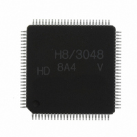
HD64F3048VTF8 Renesas Electronics America, HD64F3048VTF8 Datasheet - Page 9

HD64F3048VTF8
Manufacturer Part Number
HD64F3048VTF8
Description
IC H8 MCU FLASH 128K 100-QFP
Manufacturer
Renesas Electronics America
Series
H8® H8/300Hr
Datasheet
1.HD64F3048F16.pdf
(907 pages)
Specifications of HD64F3048VTF8
Core Processor
H8/300H
Core Size
16-Bit
Speed
8MHz
Connectivity
SCI, SmartCard
Peripherals
DMA, PWM, WDT
Number Of I /o
70
Program Memory Size
128KB (128K x 8)
Program Memory Type
FLASH
Ram Size
4K x 8
Voltage - Supply (vcc/vdd)
2.7 V ~ 5.5 V
Data Converters
A/D 8x10b; D/A 2x8b
Oscillator Type
Internal
Operating Temperature
-20°C ~ 75°C
Package / Case
100-TQFP, 100-VQFP
Lead Free Status / RoHS Status
Contains lead / RoHS non-compliant
Eeprom Size
-
Other names
HD64F3048VX8
- Current page: 9 of 907
- Download datasheet (6Mb)
Item
All
13.2.6 Serial Control
Register (SCR)
Bit 6-Receive
Interrupt Enable
(RIE)
19.5.3 Programming
Flowchart and
Sample Program
Flowchart for
Programming One
Byte
Figure 19.9
Programming
Flowchart
Page
461
606
Main Revisions for this Edition
All references to Hitachi, Hitachi, Ltd., Hitachi Semiconductors, and
other Hitachi brand names changed to Renesas Technology Corp.
Designation for categories changed from “series” to “group”
Table amended
Bit 6: RIE
0
1
Figure amended
Revision (See Manual for Details)
(clear bit of programmed block to 0)
End (1-byte data programmed)
Select program-verify mode
Clear erase block register
Enable watchdog timer
Disable watchdog timer
(PV bit = 1 in FLMCR)
Verify (read memory)
Select program mode
(P bit = 1 in FLMCR)
Clear
Wait (t
Clear PV bit
Wait (x) µs
Clear P bit
Description
Receive-data-full (RXI) and receive-error (ERI) interrupt requests
are disabled*
Receive-data-full (RXI) and receive-error (ERI) interrupt requests
are enabled
V
VS1
PP
OK
E
) µs
bit
*4
*2
*3
No good
Programming ends
Rev. 7.00 Sep 21, 2005 page vii of xxiv
Clear erase block register
(clear bit of block to be
Programming error
programmed to 0)
Clear
Clear PV bit
n
V
N?
PP
Notes: 1. Write the data to be programmed using a
Yes
E
bit
2. Set the watchdog timer overflow interval
3. Read to verify data from the memory
4. t
5. Programming time x, which is determined
byte transfer instruction.
by setting CKS2 and CKS1 to 0 and
CKS0 to 1.
using a byte transfer instruction.
z:
N:
by the initial time
increases in proportion to n. Thus, set the
initial time to 15.8 s or less to make total
programming time 1 ms or less.
VS1
Verify ends
: 4 µs
No
time does not exceed 1 ms)
5 to 10 s
6 (set N so that total programming
Double the programming
time (x
n + 1
2n
–1
(Initial value)
(n = 1 to 6),
2
n
x)
*5
Related parts for HD64F3048VTF8
Image
Part Number
Description
Manufacturer
Datasheet
Request
R

Part Number:
Description:
KIT STARTER FOR M16C/29
Manufacturer:
Renesas Electronics America
Datasheet:

Part Number:
Description:
KIT STARTER FOR R8C/2D
Manufacturer:
Renesas Electronics America
Datasheet:

Part Number:
Description:
R0K33062P STARTER KIT
Manufacturer:
Renesas Electronics America
Datasheet:

Part Number:
Description:
KIT STARTER FOR R8C/23 E8A
Manufacturer:
Renesas Electronics America
Datasheet:

Part Number:
Description:
KIT STARTER FOR R8C/25
Manufacturer:
Renesas Electronics America
Datasheet:

Part Number:
Description:
KIT STARTER H8S2456 SHARPE DSPLY
Manufacturer:
Renesas Electronics America
Datasheet:

Part Number:
Description:
KIT STARTER FOR R8C38C
Manufacturer:
Renesas Electronics America
Datasheet:

Part Number:
Description:
KIT STARTER FOR R8C35C
Manufacturer:
Renesas Electronics America
Datasheet:

Part Number:
Description:
KIT STARTER FOR R8CL3AC+LCD APPS
Manufacturer:
Renesas Electronics America
Datasheet:

Part Number:
Description:
KIT STARTER FOR RX610
Manufacturer:
Renesas Electronics America
Datasheet:

Part Number:
Description:
KIT STARTER FOR R32C/118
Manufacturer:
Renesas Electronics America
Datasheet:

Part Number:
Description:
KIT DEV RSK-R8C/26-29
Manufacturer:
Renesas Electronics America
Datasheet:

Part Number:
Description:
KIT STARTER FOR SH7124
Manufacturer:
Renesas Electronics America
Datasheet:

Part Number:
Description:
KIT STARTER FOR H8SX/1622
Manufacturer:
Renesas Electronics America
Datasheet:


