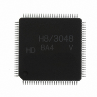
HD64F3048VTF8 Renesas Electronics America, HD64F3048VTF8 Datasheet - Page 44

HD64F3048VTF8
Manufacturer Part Number
HD64F3048VTF8
Description
IC H8 MCU FLASH 128K 100-QFP
Manufacturer
Renesas Electronics America
Series
H8® H8/300Hr
Datasheet
1.HD64F3048F16.pdf
(907 pages)
Specifications of HD64F3048VTF8
Core Processor
H8/300H
Core Size
16-Bit
Speed
8MHz
Connectivity
SCI, SmartCard
Peripherals
DMA, PWM, WDT
Number Of I /o
70
Program Memory Size
128KB (128K x 8)
Program Memory Type
FLASH
Ram Size
4K x 8
Voltage - Supply (vcc/vdd)
2.7 V ~ 5.5 V
Data Converters
A/D 8x10b; D/A 2x8b
Oscillator Type
Internal
Operating Temperature
-20°C ~ 75°C
Package / Case
100-TQFP, 100-VQFP
Lead Free Status / RoHS Status
Contains lead / RoHS non-compliant
Eeprom Size
-
Other names
HD64F3048VX8
- Current page: 44 of 907
- Download datasheet (6Mb)
Section 1 Overview
Type
Programmable
timing pattern
controller (TPC)
Serial
communication
interface (SCI)
A/D converter
D/A converter
A/D and D/A
converters
I/O ports
Rev. 7.00 Sep 21, 2005 page 18 of 878
REJ09B0259-0700
Symbol
TP
TxD
RxD
SCK
AN
ADTRG
DA
AV
AV
V
P1
P2
P3
P4
P5
REF
7
7
7
7
3
15
CC
SS
7
1
, DA
1
to P1
to P2
to P3
to P4
to P5
1
1
to AN
, TxD
to TP
, RxD
, SCK
0
0
0
0
0
0
0
0
0
0
0
Pin No.
9 to 2,
100 to 93
13, 12
15, 14
17, 16
85 to 78
9
85, 84
76
86
77
43 to 36
52 to 45
34 to 27
26 to 23,
21 to 18
56 to 53
I/O
Output
Output
Input
Input/
output
Input
Input
Output
Input
Input
Input
Input/
output
Input/
output
Input/
output
Input/
output
Input/
output
TPC output 15 to 0: Pulse output
Transmit data (channels 0 and 1):
SCI data output
Receive data (channels 0 and 1):
SCI data input
Serial clock (channels 0 and 1):
SCI clock input/output
Analog 7 to 0: Analog input pins
A/D trigger: External trigger input for
starting A/D conversion
Analog output: Analog output from the D/A
converter
Power supply pin for the A/D and D/A
converters. Connect to the system power
supply (V
D/A converters.
Ground pin for the A/D and D/A converters.
Connect to system ground (V
Reference voltage input pin for the A/D and
D/A converters. Connect to the system
power supply (V
and D/A converters.
Port 1: Eight input/output pins.
The direction of each pin can be selected in
the port 1 data direction register (P1DDR).
Port 2: Eight input/output pins.
The direction of each pin can be selected in
the port 2 data direction register (P2DDR).
Port 3: Eight input/output pins.
The direction of each pin can be selected in
the port 3 data direction register (P3DDR).
Port 4: Eight input/output pins.
The direction of each pin can be selected in
the port 4 data direction register (P4DDR).
Port 5: Four input/output pins. The direction
of each pin can be selected in the port 5
data direction register (P5DDR).
Name and Function
CC
) when not using the A/D and
CC
) when not using the A/D
SS
).
Related parts for HD64F3048VTF8
Image
Part Number
Description
Manufacturer
Datasheet
Request
R

Part Number:
Description:
KIT STARTER FOR M16C/29
Manufacturer:
Renesas Electronics America
Datasheet:

Part Number:
Description:
KIT STARTER FOR R8C/2D
Manufacturer:
Renesas Electronics America
Datasheet:

Part Number:
Description:
R0K33062P STARTER KIT
Manufacturer:
Renesas Electronics America
Datasheet:

Part Number:
Description:
KIT STARTER FOR R8C/23 E8A
Manufacturer:
Renesas Electronics America
Datasheet:

Part Number:
Description:
KIT STARTER FOR R8C/25
Manufacturer:
Renesas Electronics America
Datasheet:

Part Number:
Description:
KIT STARTER H8S2456 SHARPE DSPLY
Manufacturer:
Renesas Electronics America
Datasheet:

Part Number:
Description:
KIT STARTER FOR R8C38C
Manufacturer:
Renesas Electronics America
Datasheet:

Part Number:
Description:
KIT STARTER FOR R8C35C
Manufacturer:
Renesas Electronics America
Datasheet:

Part Number:
Description:
KIT STARTER FOR R8CL3AC+LCD APPS
Manufacturer:
Renesas Electronics America
Datasheet:

Part Number:
Description:
KIT STARTER FOR RX610
Manufacturer:
Renesas Electronics America
Datasheet:

Part Number:
Description:
KIT STARTER FOR R32C/118
Manufacturer:
Renesas Electronics America
Datasheet:

Part Number:
Description:
KIT DEV RSK-R8C/26-29
Manufacturer:
Renesas Electronics America
Datasheet:

Part Number:
Description:
KIT STARTER FOR SH7124
Manufacturer:
Renesas Electronics America
Datasheet:

Part Number:
Description:
KIT STARTER FOR H8SX/1622
Manufacturer:
Renesas Electronics America
Datasheet:


