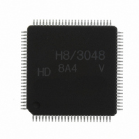
HD64F3048VTF8 Renesas Electronics America, HD64F3048VTF8 Datasheet - Page 628

HD64F3048VTF8
Manufacturer Part Number
HD64F3048VTF8
Description
IC H8 MCU FLASH 128K 100-QFP
Manufacturer
Renesas Electronics America
Series
H8® H8/300Hr
Datasheet
1.HD64F3048F16.pdf
(907 pages)
Specifications of HD64F3048VTF8
Core Processor
H8/300H
Core Size
16-Bit
Speed
8MHz
Connectivity
SCI, SmartCard
Peripherals
DMA, PWM, WDT
Number Of I /o
70
Program Memory Size
128KB (128K x 8)
Program Memory Type
FLASH
Ram Size
4K x 8
Voltage - Supply (vcc/vdd)
2.7 V ~ 5.5 V
Data Converters
A/D 8x10b; D/A 2x8b
Oscillator Type
Internal
Operating Temperature
-20°C ~ 75°C
Package / Case
100-TQFP, 100-VQFP
Lead Free Status / RoHS Status
Contains lead / RoHS non-compliant
Eeprom Size
-
Other names
HD64F3048VX8
- Current page: 628 of 907
- Download datasheet (6Mb)
Section 19 Flash Memory (H8/3048F: Dual Power Supply (V
7. During reset (when RES pin input is Low), if MD
8. Regarding 12 V application to the V
Notes: 1. Mode pin input must satisfy the mode programming setup time (t
19.4.2
When set to user program mode, the H8/3048F can erase and program its flash memory by
executing a user program. On-board updates of the on-chip flash memory can be carried out by
providing on-board circuits for supplying V
the program area.
To select user program mode, select a mode that enables the on-chip ROM (mode 5, 6, or 7) and
apply 12 V to the V
would in mode 5, 6, or 7, except for the flash memory. A watchdog timer overflow, however,
cannot output a reset signal while 12 V is applied to V
bit (RSTOE) should not be set to 1.
The flash memory cannot be read while being programmed or erased, so the update program must
either be stored in external memory, or transferred temporarily to the RAM area and executed in
RAM.
Rev. 7.00 Sep 21, 2005 page 602 of 878
REJ09B0259-0700
versa, by instantaneous transfer to 5 V input, the personal computer switches to operation
mode. As a result, the address port or bus control output signal (AS, RD, HWR, LWR) status
changes, so do not these pins as output signals during reset, as the personal computer internal
section needs to be shut down.
exceed the maximum rating of 13 V. Also, be sure to connect bypass capacitors to the V
MD
boot mode will not operate correctly. In addition, during boot program operation or writing
and erasing the flash memory, do not interrupt V
2
2. For notes on applying and cutting V
pins *
User Program Mode
the reset release timing. When 12 V is applied to or disconnected from the MD
delay occurs in the fall and rise waveforms due to the influence of the pull-up/pull-
down resistor connected to the MD
delay must be confirmed with the actual waveform on the board.
Programming and Erasing Precautions (Dual-Power Supply).”
1
.
PP
pin. In this mode, the on-chip peripheral modules operate as they normally
PP
and MD
PP
and data, and storing an update program in part of
2
PP
pin, etc. For reset release timing, therefore, this
, refer to 19.8, note (4) of “Flash Memory
2
pins, insure that peak overshoot does not
2
PP
pin input changes from 0 V to 12 V or vice
PP
. The watchdog timer’s reset output enable
*
2
.
PP
= 12 V))
MDS
) with respect to
2
pin, a
pp
and
Related parts for HD64F3048VTF8
Image
Part Number
Description
Manufacturer
Datasheet
Request
R

Part Number:
Description:
KIT STARTER FOR M16C/29
Manufacturer:
Renesas Electronics America
Datasheet:

Part Number:
Description:
KIT STARTER FOR R8C/2D
Manufacturer:
Renesas Electronics America
Datasheet:

Part Number:
Description:
R0K33062P STARTER KIT
Manufacturer:
Renesas Electronics America
Datasheet:

Part Number:
Description:
KIT STARTER FOR R8C/23 E8A
Manufacturer:
Renesas Electronics America
Datasheet:

Part Number:
Description:
KIT STARTER FOR R8C/25
Manufacturer:
Renesas Electronics America
Datasheet:

Part Number:
Description:
KIT STARTER H8S2456 SHARPE DSPLY
Manufacturer:
Renesas Electronics America
Datasheet:

Part Number:
Description:
KIT STARTER FOR R8C38C
Manufacturer:
Renesas Electronics America
Datasheet:

Part Number:
Description:
KIT STARTER FOR R8C35C
Manufacturer:
Renesas Electronics America
Datasheet:

Part Number:
Description:
KIT STARTER FOR R8CL3AC+LCD APPS
Manufacturer:
Renesas Electronics America
Datasheet:

Part Number:
Description:
KIT STARTER FOR RX610
Manufacturer:
Renesas Electronics America
Datasheet:

Part Number:
Description:
KIT STARTER FOR R32C/118
Manufacturer:
Renesas Electronics America
Datasheet:

Part Number:
Description:
KIT DEV RSK-R8C/26-29
Manufacturer:
Renesas Electronics America
Datasheet:

Part Number:
Description:
KIT STARTER FOR SH7124
Manufacturer:
Renesas Electronics America
Datasheet:

Part Number:
Description:
KIT STARTER FOR H8SX/1622
Manufacturer:
Renesas Electronics America
Datasheet:


