HD64F3048VTF8 Renesas Electronics America, HD64F3048VTF8 Datasheet - Page 366
HD64F3048VTF8
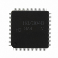
Manufacturer Part Number
HD64F3048VTF8
Description
IC H8 MCU FLASH 128K 100-QFP
Manufacturer
Renesas Electronics America
Series
H8® H8/300Hr
Datasheet
1.HD64F3048F16.pdf
(907 pages)
Specifications of HD64F3048VTF8
Core Processor
H8/300H
Core Size
16-Bit
Speed
8MHz
Connectivity
SCI, SmartCard
Peripherals
DMA, PWM, WDT
Number Of I /o
70
Program Memory Size
128KB (128K x 8)
Program Memory Type
FLASH
Ram Size
4K x 8
Voltage - Supply (vcc/vdd)
2.7 V ~ 5.5 V
Data Converters
A/D 8x10b; D/A 2x8b
Oscillator Type
Internal
Operating Temperature
-20°C ~ 75°C
Package / Case
100-TQFP, 100-VQFP
Lead Free Status / RoHS Status
Contains lead / RoHS non-compliant
Eeprom Size
-
Other names
HD64F3048VX8


Section 10 16-Bit Integrated Timer Unit (ITU)
general register. The corresponding IMFA or IMFB flag in TSR is set to 1 at the same time. The
valid edge or edges of the input capture signal are selected in TIOR.
TIOR settings are ignored in PWM mode, complementary PWM mode, and reset-synchronized
PWM mode.
General registers are linked to the CPU by an internal 16-bit bus and can be written or read by
either word access or byte access.
General registers are initialized to the output compare function (with no output signal) by a reset
and in standby mode. The initial value is H'FFFF.
10.2.9
The buffer registers are 16-bit registers. The ITU has four buffer registers, two each in channels 3
and 4.
Channel
3
4
A buffer register is a 16-bit readable/writable register that is used when buffering is selected.
Buffering can be selected independently by bits BFB4, BFA4, BFB3, and BFA3 in TFCR.
The buffer register and general register operate as a pair. When the general register functions as an
output compare register, the buffer register functions as an output compare buffer register. When
the general register functions as an input capture register, the buffer register functions as an input
capture buffer register.
Rev. 7.00 Sep 21, 2005 page 340 of 878
REJ09B0259-0700
Bit
Initial value
Read/Write
Buffer Registers (BRA, BRB)
Abbreviation
BRA3, BRB3
BRA4, BRB4
R/W
15
1
R/W
14
1
R/W
13
1
R/W
12
1
Function
Used for buffering
R/W
11
When the corresponding GRA or GRB functions as an
output compare register, BRA or BRB can function as an
output compare buffer register: the BRA or BRB value is
automatically transferred to GRA or GRB at compare match
When the corresponding GRA or GRB functions as an input
capture register, BRA or BRB can function as an input
capture buffer register: the GRA or GRB value is
automatically transferred to BRA or BRB at input capture
1
R/W
10
1
R/W
9
1
R/W
8
1
R/W
7
1
R/W
6
1
R/W
5
1
R/W
4
1
R/W
3
1
R/W
2
1
R/W
1
1
R/W
0
1
Related parts for HD64F3048VTF8
Image
Part Number
Description
Manufacturer
Datasheet
Request
R


Part Number:
Description:
KIT STARTER FOR M16C/29
Manufacturer:
Renesas Electronics America
Datasheet:

Part Number:
Description:
KIT STARTER FOR R8C/2D
Manufacturer:
Renesas Electronics America
Datasheet:

Part Number:
Description:
R0K33062P STARTER KIT
Manufacturer:
Renesas Electronics America
Datasheet:

Part Number:
Description:
KIT STARTER FOR R8C/23 E8A
Manufacturer:
Renesas Electronics America
Datasheet:

Part Number:
Description:
KIT STARTER FOR R8C/25
Manufacturer:
Renesas Electronics America
Datasheet:

Part Number:
Description:
KIT STARTER H8S2456 SHARPE DSPLY
Manufacturer:
Renesas Electronics America
Datasheet:

Part Number:
Description:
KIT STARTER FOR R8C38C
Manufacturer:
Renesas Electronics America
Datasheet:

Part Number:
Description:
KIT STARTER FOR R8C35C
Manufacturer:
Renesas Electronics America
Datasheet:

Part Number:
Description:
KIT STARTER FOR R8CL3AC+LCD APPS
Manufacturer:
Renesas Electronics America
Datasheet:
Part Number:
Description:
KIT STARTER FOR RX610
Manufacturer:
Renesas Electronics America
Datasheet:

Part Number:
Description:
KIT STARTER FOR R32C/118
Manufacturer:
Renesas Electronics America
Datasheet:

Part Number:
Description:
KIT DEV RSK-R8C/26-29
Manufacturer:
Renesas Electronics America
Datasheet:

Part Number:
Description:
KIT STARTER FOR SH7124
Manufacturer:
Renesas Electronics America
Datasheet:

Part Number:
Description:
KIT STARTER FOR H8SX/1622
Manufacturer:
Renesas Electronics America
Datasheet: