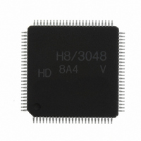
HD64F3048VTF8 Renesas Electronics America, HD64F3048VTF8 Datasheet - Page 209

HD64F3048VTF8
Manufacturer Part Number
HD64F3048VTF8
Description
IC H8 MCU FLASH 128K 100-QFP
Manufacturer
Renesas Electronics America
Series
H8® H8/300Hr
Datasheet
1.HD64F3048F16.pdf
(907 pages)
Specifications of HD64F3048VTF8
Core Processor
H8/300H
Core Size
16-Bit
Speed
8MHz
Connectivity
SCI, SmartCard
Peripherals
DMA, PWM, WDT
Number Of I /o
70
Program Memory Size
128KB (128K x 8)
Program Memory Type
FLASH
Ram Size
4K x 8
Voltage - Supply (vcc/vdd)
2.7 V ~ 5.5 V
Data Converters
A/D 8x10b; D/A 2x8b
Oscillator Type
Internal
Operating Temperature
-20°C ~ 75°C
Package / Case
100-TQFP, 100-VQFP
Lead Free Status / RoHS Status
Contains lead / RoHS non-compliant
Eeprom Size
-
Other names
HD64F3048VX8
- Current page: 209 of 907
- Download datasheet (6Mb)
Example 4: Connection to Multiple 4-Mbit DRAM Chips (16-Mbyte Mode): Figure 7.13
shows an example of interconnections to two 2CAS 4-Mbit DRAM chips, and the corresponding
address map. Up to four DRAM chips can be connected to area 3 by decoding upper address bits
A
Figure 7.14 shows a setup procedure to be followed by a program for this example. The DRAM in
this example has 9-bit row addresses and 9-bit column addresses. Both chips must be refreshed
simultaneously, so the RFSH pin must be used.
19
Figure 7.13 Interconnections and Address Map for Multiple 2CAS
and A
20
.
H8/3048 Group
H'600000
H'67FFFF
H'680000
H'6FFFFF
H'700000
H'7FFFFF
D
A to A
15
9
RFSH
HWR
to D
LWR
CS
A
RD
19
1
3
0
DRAM area
DRAM area
Not used
No. 1
No. 2
a. Interconnections (example)
b. Address map
(Example)
Area 3 (16-Mbyte mode)
Rev. 7.00 Sep 21, 2005 page 183 of 878
2
row address, 9-bit column
address, and
CAS
A to A
RAS
UCAS
LCAS
WE
OE
I/O
A to A
RAS
UCAS
LCAS
WE
OE
I/O
8
8
15
15
CAS 4-Mbit DRAM Chips
CAS
CAS
4-Mbit DRAM with 9-bit
Section 7 Refresh Controller
to I/O
to I/O
0
0
0
0
16-bit organization
REJ09B0259-0700
No. 1
No. 2
Related parts for HD64F3048VTF8
Image
Part Number
Description
Manufacturer
Datasheet
Request
R

Part Number:
Description:
KIT STARTER FOR M16C/29
Manufacturer:
Renesas Electronics America
Datasheet:

Part Number:
Description:
KIT STARTER FOR R8C/2D
Manufacturer:
Renesas Electronics America
Datasheet:

Part Number:
Description:
R0K33062P STARTER KIT
Manufacturer:
Renesas Electronics America
Datasheet:

Part Number:
Description:
KIT STARTER FOR R8C/23 E8A
Manufacturer:
Renesas Electronics America
Datasheet:

Part Number:
Description:
KIT STARTER FOR R8C/25
Manufacturer:
Renesas Electronics America
Datasheet:

Part Number:
Description:
KIT STARTER H8S2456 SHARPE DSPLY
Manufacturer:
Renesas Electronics America
Datasheet:

Part Number:
Description:
KIT STARTER FOR R8C38C
Manufacturer:
Renesas Electronics America
Datasheet:

Part Number:
Description:
KIT STARTER FOR R8C35C
Manufacturer:
Renesas Electronics America
Datasheet:

Part Number:
Description:
KIT STARTER FOR R8CL3AC+LCD APPS
Manufacturer:
Renesas Electronics America
Datasheet:

Part Number:
Description:
KIT STARTER FOR RX610
Manufacturer:
Renesas Electronics America
Datasheet:

Part Number:
Description:
KIT STARTER FOR R32C/118
Manufacturer:
Renesas Electronics America
Datasheet:

Part Number:
Description:
KIT DEV RSK-R8C/26-29
Manufacturer:
Renesas Electronics America
Datasheet:

Part Number:
Description:
KIT STARTER FOR SH7124
Manufacturer:
Renesas Electronics America
Datasheet:

Part Number:
Description:
KIT STARTER FOR H8SX/1622
Manufacturer:
Renesas Electronics America
Datasheet:


