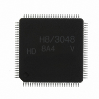
HD64F3048VTF8 Renesas Electronics America, HD64F3048VTF8 Datasheet - Page 556

HD64F3048VTF8
Manufacturer Part Number
HD64F3048VTF8
Description
IC H8 MCU FLASH 128K 100-QFP
Manufacturer
Renesas Electronics America
Series
H8® H8/300Hr
Datasheet
1.HD64F3048F16.pdf
(907 pages)
Specifications of HD64F3048VTF8
Core Processor
H8/300H
Core Size
16-Bit
Speed
8MHz
Connectivity
SCI, SmartCard
Peripherals
DMA, PWM, WDT
Number Of I /o
70
Program Memory Size
128KB (128K x 8)
Program Memory Type
FLASH
Ram Size
4K x 8
Voltage - Supply (vcc/vdd)
2.7 V ~ 5.5 V
Data Converters
A/D 8x10b; D/A 2x8b
Oscillator Type
Internal
Operating Temperature
-20°C ~ 75°C
Package / Case
100-TQFP, 100-VQFP
Lead Free Status / RoHS Status
Contains lead / RoHS non-compliant
Eeprom Size
-
Other names
HD64F3048VX8
- Current page: 556 of 907
- Download datasheet (6Mb)
Section 14 Smart Card Interface
Examples of Operation in GSM Mode: When switching between smart card interface mode and
software standby mode, use the following procedures to maintain the clock duty cycle.
Use the following procedure to secure the clock duty cycle after powering on.
1. The initial state is port input and high impedance. Use pull-up or pull-down resistors to fix the
2. Fix at the output specified by the CKE1 bit in SCR.
3. Set SMR and SCMR, and switch to smart card interface mode operation.
4. Set the CKE0 bit in SCR to 1 to start clock output.
Rev. 7.00 Sep 21, 2005 page 530 of 878
REJ09B0259-0700
Switching from smart card interface mode to software standby mode
1. Set the P94 data register (DR) and data direction register (DDR) to the values for the fixed
2. Write 0 to the TE and RE bits in the serial control register (SCR) to stop transmit/receive
3. Write 0 to the CKE0 bit in SCR to stop the clock.
4. Wait for one serial clock cycle. During this period, the duty cycle is preserved and clock
5. Write H'00 to the serial mode register (SMR) and smart card mode register (SCMR).
6. Make the transition to the software standby state.
Returning from software standby mode to smart card interface mode
1. Clear the software standby state.
2. Set the CKE1 bit in SCR to the value for the fixed output state at the start of software
3. Set smart card interface mode and output the clock. Clock signal generation is started with
potential.
output state in software standby mode.
operations. At the same time, set the CKE1 bit to the value for the fixed output state in
software standby mode.
output is fixed at the specified level.
standby (the current P94 pin state).
the normal duty cycle.
Figure 14.9 Procedure for Stopping and Restarting the Clock
(1)(2)(3)
Normal operation
(4) (5)(6)
Software standby
mode
(1) (2)(3)
Normal operation
Related parts for HD64F3048VTF8
Image
Part Number
Description
Manufacturer
Datasheet
Request
R

Part Number:
Description:
KIT STARTER FOR M16C/29
Manufacturer:
Renesas Electronics America
Datasheet:

Part Number:
Description:
KIT STARTER FOR R8C/2D
Manufacturer:
Renesas Electronics America
Datasheet:

Part Number:
Description:
R0K33062P STARTER KIT
Manufacturer:
Renesas Electronics America
Datasheet:

Part Number:
Description:
KIT STARTER FOR R8C/23 E8A
Manufacturer:
Renesas Electronics America
Datasheet:

Part Number:
Description:
KIT STARTER FOR R8C/25
Manufacturer:
Renesas Electronics America
Datasheet:

Part Number:
Description:
KIT STARTER H8S2456 SHARPE DSPLY
Manufacturer:
Renesas Electronics America
Datasheet:

Part Number:
Description:
KIT STARTER FOR R8C38C
Manufacturer:
Renesas Electronics America
Datasheet:

Part Number:
Description:
KIT STARTER FOR R8C35C
Manufacturer:
Renesas Electronics America
Datasheet:

Part Number:
Description:
KIT STARTER FOR R8CL3AC+LCD APPS
Manufacturer:
Renesas Electronics America
Datasheet:

Part Number:
Description:
KIT STARTER FOR RX610
Manufacturer:
Renesas Electronics America
Datasheet:

Part Number:
Description:
KIT STARTER FOR R32C/118
Manufacturer:
Renesas Electronics America
Datasheet:

Part Number:
Description:
KIT DEV RSK-R8C/26-29
Manufacturer:
Renesas Electronics America
Datasheet:

Part Number:
Description:
KIT STARTER FOR SH7124
Manufacturer:
Renesas Electronics America
Datasheet:

Part Number:
Description:
KIT STARTER FOR H8SX/1622
Manufacturer:
Renesas Electronics America
Datasheet:


