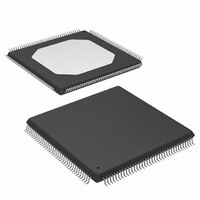
XC3S200-4TQG144I Xilinx Inc, XC3S200-4TQG144I Datasheet - Page 103

XC3S200-4TQG144I
Manufacturer Part Number
XC3S200-4TQG144I
Description
FPGA Spartan®-3 Family 200K Gates 4320 Cells 630MHz 90nm Technology 1.2V 144-Pin TQFP
Manufacturer
Xilinx Inc
Series
Spartan™-3r
Datasheet
1.XC3S50-4VQG100C.pdf
(217 pages)
Specifications of XC3S200-4TQG144I
Package
144TQFP
Family Name
Spartan®-3
Device Logic Units
4320
Device System Gates
200000
Maximum Internal Frequency
630 MHz
Typical Operating Supply Voltage
1.2 V
Maximum Number Of User I/os
97
Ram Bits
221184
Package / Case
144-TQFP, 144-VQFP
Mounting Type
Surface Mount
Voltage - Supply
1.14 V ~ 3.465 V
Operating Temperature
-40°C ~ 100°C
Number Of I /o
97
Number Of Logic Elements/cells
*
Number Of Gates
*
Lead Free Status / RoHS Status
Lead free / RoHS Compliant
Available stocks
Company
Part Number
Manufacturer
Quantity
Price
Company:
Part Number:
XC3S200-4TQG144I
Manufacturer:
XILINX
Quantity:
1 029
Table 69: Spartan-3 FPGA Pin Definitions (Continued)
DS099-4 (v2.5) December 4, 2009
Product Specification
DONE
M0, M1, M2
HSWAP_EN
JTAG: JTAG interface pins (pull-up resistor to VCCAUX always active during configuration, regardless of HSWAP_EN pin)
TCK
TDI
TMS
TDO
VCCO: I/O bank output voltage supply pins
VCCO_#
Pin Name
R
Bidirectional with open-drain
or totem-pole Output
Input
Input
Input
Input
Input
Output
Supply
Direction
www.xilinx.com
Configuration Done, Delay Start-up Sequence:
A Low-to-High output transition on this bidirectional pin signals the
end of the configuration process.
The FPGA produces a Low-to-High transition on this pin to
indicate that the configuration process is complete. The DriveDone
bitstream generation option defines whether this pin functions as
a totem-pole output that actively drives High or as an open-drain
output. An open-drain output requires a pull-up resistor to produce
a High logic level. The open-drain option permits the DONE lines
of multiple FPGAs to be tied together, so that the common node
transitions High only after all of the FPGAs have completed
configuration. Externally holding the open-drain output Low delays
the start-up sequence, which marks the transition to user mode.
Configuration Mode Selection:
These inputs select the configuration mode. The logic levels
applied to the mode pins are sampled on the rising edge of INIT_B.
See
VCCAUX during configuration, making Slave Serial the default
configuration mode.
Disable Pull-up Resistors During Configuration:
A Low on this pin enables pull-up resistors on all pins that are not
actively involved in the configuration process. A High value
disables all pull-ups, allowing the non-configuration pins to float.
JTAG Test Clock:
The TCK clock signal synchronizes all JTAG port operations. This
pin has an internal pull-up resistor to VCCAUX during
configuration.
JTAG Test Data Input:
TDI is the serial data input for all JTAG instruction and data
registers. This pin has an internal pull-up resistor to VCCAUX
during configuration.
JTAG Test Mode Select:
The serial TMS input controls the operation of the JTAG port. This
pin has an internal pull-up resistor to VCCAUX during
configuration.
JTAG Test Data Output:
TDO is the serial data output for all JTAG instruction and data
registers. This pin has an internal pull-up resistor to VCCAUX
during configuration.
Power Supply for Output Buffer Drivers (per bank):
These pins power the output drivers within a specific I/O bank.
Table
74. These pins have an internal pull-up resistor to
Spartan-3 FPGA Family: Pinout Descriptions
Description
103


