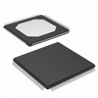
XC3S200-4TQG144I Xilinx Inc, XC3S200-4TQG144I Datasheet - Page 88

XC3S200-4TQG144I
Manufacturer Part Number
XC3S200-4TQG144I
Description
FPGA Spartan®-3 Family 200K Gates 4320 Cells 630MHz 90nm Technology 1.2V 144-Pin TQFP
Manufacturer
Xilinx Inc
Series
Spartan™-3r
Datasheet
1.XC3S50-4VQG100C.pdf
(217 pages)
Specifications of XC3S200-4TQG144I
Package
144TQFP
Family Name
Spartan®-3
Device Logic Units
4320
Device System Gates
200000
Maximum Internal Frequency
630 MHz
Typical Operating Supply Voltage
1.2 V
Maximum Number Of User I/os
97
Ram Bits
221184
Package / Case
144-TQFP, 144-VQFP
Mounting Type
Surface Mount
Voltage - Supply
1.14 V ~ 3.465 V
Operating Temperature
-40°C ~ 100°C
Number Of I /o
97
Number Of Logic Elements/cells
*
Number Of Gates
*
Lead Free Status / RoHS Status
Lead free / RoHS Compliant
Available stocks
Company
Part Number
Manufacturer
Quantity
Price
Company:
Part Number:
XC3S200-4TQG144I
Manufacturer:
XILINX
Quantity:
1 029
- Current page: 88 of 217
- Download datasheet (6Mb)
Spartan-3 FPGA Family: DC and Switching Characteristics
Table 58: Switching Characteristics for the DLL (Continued)
Notes:
1.
2.
3.
4.
5.
Digital Frequency Synthesizer (DFS)
Table 59: Recommended Operating Conditions for the DFS
88
Notes:
1.
2.
3.
Lock Time
LOCK_DLL
Delay Lines
DCM_TAP
Input Frequency Ranges
F
Input Clock Jitter Tolerance
CLKIN_CYC_JITT_FX_LF
CLKIN_CYC_JITT_FX_HF
CLKIN_PER_JITT_FX
CLKIN
The numbers in this table are based on the operating conditions set forth in
DLL specifications apply when any of the DLL outputs (CLK0, CLK90, CLK180, CLK270, CLK2X, CLK2X180, or CLKDV) are in use.
Only mask revision ‘E’ and later devices (see
feedback using the CLK2X output. For all other Spartan-3 devices, use feedback from the CLK0 output (instead of the CLK2X output) and set the
CLK_FEEDBACK attribute to 1X.
Indicates the maximum amount of output jitter that the DCM adds to the jitter on the CLKIN input.
This specification only applies if the attribute DUTY_CYCLE_CORRECTION = TRUE.
DFS specifications apply when either of the DFS outputs (CLKFX or CLKFX180) are used.
If both DFS and DLL outputs are used on the same DCM, follow the more restrictive CLKIN_FREQ_DLL specifications in
CLKIN input jitter beyond these limits may cause the DCM to lose lock.
Symbol
CLKIN_FREQ_FX
Symbol
(2)
(3)
When using the DLL alone: The
time from deassertion at the
DCM’s Reset input to the rising
transition at its LOCKED output.
When the DCM is locked, the
CLKIN and CLKFB signals are
in phase
Delay tap resolution
Description
Frequency for the CLKIN input
Cycle-to-cycle jitter at the
CLKIN input
Period jitter at the CLKIN input
Mask and Fab Revisions, page
Description
www.xilinx.com
18 MHz < F
30 MHz < F
40 MHz < F
50 MHz < F
Frequency Mode /
F
F
CLKIN
CLKIN
Table 31
CLKIN
CLKIN
CLKIN
CLKIN
All
> 60 MHz
55) and all revisions of the XC3S50 and the XC3S1000 support DLL
Range
Frequency
Mode
< 30 MHz
< 40 MHz
< 50 MHz
< 60 MHz
High
Low
All
All
and
Table
57.
Min
Device
1
-
-
-
All
All
-5
±
±
Max
Speed Grade
280
DS099-3 (v2.5) December 4, 2009
±
300
150
30.0
Min
1
-
-
-
-
-
-5
Speed Grade
Max
2.88
2.16
1.20
0.60
0.48
60.0
Min
1
-
-
-
Product Specification
30.0
-4
Min
-
-
-
-
-
±
±
Max
280
-4
±
300
150
1
Max
2.88
2.16
1.20
0.60
0.48
60.0
Table
Units
MHz
Units
ps
ps
ns
ms
ms
ms
ms
ms
ps
57.
R
Related parts for XC3S200-4TQG144I
Image
Part Number
Description
Manufacturer
Datasheet
Request
R

Part Number:
Description:
IC SPARTAN-3 FPGA 200K 208-PQFP
Manufacturer:
Xilinx Inc
Datasheet:

Part Number:
Description:
IC SPARTAN-3 FPGA 200K 144-TQFP
Manufacturer:
Xilinx Inc
Datasheet:

Part Number:
Description:
SPARTAN-3A FPGA 200K STD 100VQFP
Manufacturer:
Xilinx Inc
Datasheet:

Part Number:
Description:
SPARTAN-3A FPGA 200K STD 100VQFP
Manufacturer:
Xilinx Inc

Part Number:
Description:
SPARTAN-3A FPGA 200K 144-TQFP
Manufacturer:
Xilinx Inc
Datasheet:

Part Number:
Description:
SPARTAN3A FPGA 200K STD 256FTBGA
Manufacturer:
Xilinx Inc
Datasheet:

Part Number:
Description:
IC FPGA SPARTAN 3 144TQFP
Manufacturer:
Xilinx Inc
Datasheet:

Part Number:
Description:
FLASH PROMS
Manufacturer:
Xilinx Inc
Datasheet:

Part Number:
Description:
FIELD PROGRAMMABLE G A
Manufacturer:
Xilinx Inc
Datasheet:

Part Number:
Description:
FPGA Spartan®-3 Family 200K Gates 4320 Cells 630MHz 90nm Technology 1.2V 256-Pin FTBGA
Manufacturer:
Xilinx Inc
Datasheet:

Part Number:
Description:
FPGA Spartan®-3 Family 200K Gates 4320 Cells 630MHz 90nm Technology 1.2V 256-Pin FTBGA
Manufacturer:
Xilinx Inc
Datasheet:

Part Number:
Description:
FPGA Spartan®-3 Family 200K Gates 4320 Cells 630MHz 90nm Technology 1.2V 208-Pin PQFP
Manufacturer:
Xilinx Inc
Datasheet:

Part Number:
Description:
FPGA Spartan®-3 Family 200K Gates 4320 Cells 630MHz 90nm Technology 1.2V 208-Pin PQFP
Manufacturer:
Xilinx Inc
Datasheet:

Part Number:
Description:
FPGA Spartan®-3 Family 200K Gates 4320 Cells 630MHz 90nm Technology 1.2V 144-Pin TQFP
Manufacturer:
Xilinx Inc
Datasheet:

Part Number:
Description:
FPGA Spartan®-3 Family 200K Gates 4320 Cells 630MHz 90nm Technology 1.2V 100-Pin VTQFP
Manufacturer:
Xilinx Inc
Datasheet:


