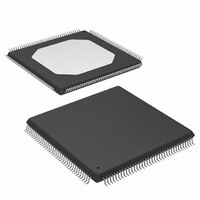
XC3S200-4TQG144I Xilinx Inc, XC3S200-4TQG144I Datasheet - Page 37

XC3S200-4TQG144I
Manufacturer Part Number
XC3S200-4TQG144I
Description
FPGA Spartan®-3 Family 200K Gates 4320 Cells 630MHz 90nm Technology 1.2V 144-Pin TQFP
Manufacturer
Xilinx Inc
Series
Spartan™-3r
Datasheet
1.XC3S50-4VQG100C.pdf
(217 pages)
Specifications of XC3S200-4TQG144I
Package
144TQFP
Family Name
Spartan®-3
Device Logic Units
4320
Device System Gates
200000
Maximum Internal Frequency
630 MHz
Typical Operating Supply Voltage
1.2 V
Maximum Number Of User I/os
97
Ram Bits
221184
Package / Case
144-TQFP, 144-VQFP
Mounting Type
Surface Mount
Voltage - Supply
1.14 V ~ 3.465 V
Operating Temperature
-40°C ~ 100°C
Number Of I /o
97
Number Of Logic Elements/cells
*
Number Of Gates
*
Lead Free Status / RoHS Status
Lead free / RoHS Compliant
Available stocks
Company
Part Number
Manufacturer
Quantity
Price
Company:
Part Number:
XC3S200-4TQG144I
Manufacturer:
XILINX
Quantity:
1 029
Digital Frequency Synthesizer (DFS)
The DFS component generates clock signals the frequency
of which is a product of the clock frequency at the CLKIN
input and a ratio of two user-determined integers. Because
of the wide range of possible output frequencies such a ratio
permits, the DFS feature provides still further flexibility than
the DLL’s basic synthesis options as described in the pre-
ceding section. The DFS component’s two dedicated out-
puts, CLKFX and CLKFX180, are defined in
The signal at the CLKFX180 output is essentially an inver-
sion of the CLKFX signal. These two outputs always exhibit
a 50% duty cycle. This is true even when the CLKIN signal
does not. These DFS clock outputs are driven at the same
time as the DLL’s seven clock outputs.
The numerator of the ratio is the integer value assigned to
the attribute CLKFX_MULTIPLY and the denominator is the
integer value assigned to the attribute CLKFX_DIVIDE.
These attributes are described in
The output frequency (f
tion of the incoming clock frequency (f
Regarding the two attributes, it is possible to assign any
combination of integer values, provided that two conditions
are met:
1. The two values fall within their corresponding ranges,
2. The f
For example, if CLKFX_MULTIPLY = 5 and CLKFX_DIVIDE
= 3, then the frequency of the output clock signal would be
5/3 that of the input clock signal.
DFS Frequency Modes
The DFS supports two operating modes, High Frequency
and Low Frequency, with each specified over a different
clock frequency range. The DFS_FREQUENCY_MODE
attribute chooses between the two modes. When the
attribute is set to LOW, the Low Frequency mode permits
Table 17: DFS Attributes
Table 18: DFS Signals
DS099-2 (v2.5) December 4, 2009
Product Specification
DFS_FREQUENCY_MODE
CLKFX_MULTIPLY
CLKFX_DIVIDE
CLKFX
CLKFX180
f
CLKFX
Signal
as specified in
expression accords with the DCM’s operating frequency
specifications.
= f
CLKFX
Attribute
CLKIN
R
Direction
frequency calculated from the above
*(CLKFX_MULTIPLY/CLKFX_DIVIDE) (3)
Output
Output
Table
CLKFX
17.
Multiplies the CLKIN frequency by the attribute-value ratio
(CLKFX_MULTIPLY/CLKFX_DIVIDE) to generate a clock signal with a new target frequency.
Generates a clock signal with same frequency as CLKFX, only shifted 180° out-of-phase.
) can be expressed as a func-
Frequency multiplier constant
Chooses between High Frequency and Low Frequency modes
Frequency divisor constant
Table
CLKIN
17.
) as follows:
Table
18.
www.xilinx.com
Description
the two DFS outputs to operate over a low-to-moderate fre-
quency range. When the attribute is set to HIGH, the High
Frequency mode allows both these outputs to operate at the
highest possible frequencies.
DFS With or Without the DLL
The DFS component can be used with or without the DLL
component:
Without the DLL, the DFS component multiplies or divides
the CLKIN signal frequency according to the respective
CLKFX_MULTIPLY and CLKFX_DIVIDE values, generating
a clock with the new target frequency on the CLKFX and
CLKFX180 outputs. Though classified as belonging to the
DLL component, the CLKIN input is shared with the DFS
component. This case does not employ feedback loop;
therefore, it cannot correct for clock distribution delay.
With the DLL, the DFS operates as described in the preced-
ing case, only with the additional benefit of eliminating the
clock distribution delay. In this case, a feedback loop from
the CLK0 output to the CLKFB input must be present.
The DLL and DFS components work together to achieve
this phase correction as follows: Given values for the
CLKFX_MULTIPLY and CLKFX_DIVIDE attributes, the DLL
selects the delay element for which the output clock edge
coincides with the input clock edge whenever mathemati-
cally possible. For example, when CLKFX_MULTIPLY = 5
and CLKFX_DIVIDE = 3, the input and output clock edges
will coincide every three input periods, which is equivalent in
time to five output periods.
Smaller CLKFX_MULTIPLY and CLKFX_DIVIDE values
achieve faster lock times. With no factors common to the
two attributes, alignment will occur once with every number
of cycles equal to the CLKFX_DIVIDE value. Therefore, it is
recommended that the user reduce these values by factor-
ing
CLKFX_MULTIPLY = 9 and CLKFX_DIVIDE = 6, removing
a factor of three yields CLKFX_MULTIPLY = 3 and
CLKFX_DIVIDE = 2. While both value-pairs will result in the
multiplication of clock frequency by 3/2, the latter value-pair
will enable the DLL to lock more quickly.
Description
wherever
Spartan-3 FPGA Family: Functional Description
possible.
For
Low, High
Integer from 2 to 32
Integer from 1 to 32
example,
Values
given
37


