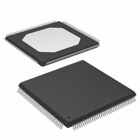
XC3S200-4TQG144I Xilinx Inc, XC3S200-4TQG144I Datasheet - Page 177

XC3S200-4TQG144I
Manufacturer Part Number
XC3S200-4TQG144I
Description
FPGA Spartan®-3 Family 200K Gates 4320 Cells 630MHz 90nm Technology 1.2V 144-Pin TQFP
Manufacturer
Xilinx Inc
Series
Spartan™-3r
Datasheet
1.XC3S50-4VQG100C.pdf
(217 pages)
Specifications of XC3S200-4TQG144I
Package
144TQFP
Family Name
Spartan®-3
Device Logic Units
4320
Device System Gates
200000
Maximum Internal Frequency
630 MHz
Typical Operating Supply Voltage
1.2 V
Maximum Number Of User I/os
97
Ram Bits
221184
Package / Case
144-TQFP, 144-VQFP
Mounting Type
Surface Mount
Voltage - Supply
1.14 V ~ 3.465 V
Operating Temperature
-40°C ~ 100°C
Number Of I /o
97
Number Of Logic Elements/cells
*
Number Of Gates
*
Lead Free Status / RoHS Status
Lead free / RoHS Compliant
Available stocks
Company
Part Number
Manufacturer
Quantity
Price
Company:
Part Number:
XC3S200-4TQG144I
Manufacturer:
XILINX
Quantity:
1 029
- Current page: 177 of 217
- Download datasheet (6Mb)
Table 102: FG676 Package Pinout (Continued)
User I/Os by Bank
Table 103
tributed between the eight I/O banks for the XC3S1000 in
the FG676 package. Similarly,
Table 103: User I/Os Per Bank for XC3S1000 in FG676 Package
DS099-4 (v2.5) December 4, 2009
Product Specification
Notes:
1.
2.
3.
Bank
VCC
VCC
VCC
VCC
VCC
VCC
VCC
VCC
AUX
AUX
AUX
AUX
AUX
AUX
AUX
AUX
XC3S1500 balls D25 and F25 are not VREF pins although they are designated as such. If a design uses an IOSTANDARD requiring VREF in bank
2 then apply the workaround in
XC3S4000 is pin compatible with XC3S2000 but uses alternate differential pair labeling on six package balls (H20, H21, H22, H23, H24, J21).
XC3S5000 is pin compatible with XC3S4000 but uses alternate differential pair functionality on fifteen package balls (A3, A8, B8, B18, C4, C8, C18,
D8, D18, E8, E18, H23, H24, AB9, and AC9).
Bottom
Edge
Right
Left
M0
M1
M2
PROG_B
TCK
TDI
TDO
TMS
Top
indicates how the available user-I/O pins are dis-
XC3S1000
Pin Name
R
Bank
I/O
0
1
2
3
4
5
6
7
M0
M1
M2
PROG_B
TCK
TDI
TDO
TMS
Answer Record 20519
XC3S1500
Pin Name
Table 104
Maximum
I/O
49
50
48
48
50
50
48
48
shows how the
M0
M1
M2
PROG_B
TCK
TDI
TDO
TMS
XC3S2000
Pin Name
.
I/O
40
41
41
41
35
35
41
41
www.xilinx.com
available user-I/O pins are distributed between the eight I/O
banks for the XC3S1500 in the FG676 package. Finally,
Table 105
XC3S4000, and XC3S5000 in the FG676 package.
M0
M1
M2
PROG_B
TCK
TDI
TDO
TMS
DUAL
0
0
0
0
6
6
0
0
XC3S4000
Pin Name
All Possible I/O Pins by Type
shows the same information for the XC3S2000,
Spartan-3 FPGA Family: Pinout Descriptions
DCI
2
2
2
2
2
2
2
2
M0
M1
M2
PROG_B
TCK
TDI
TDO
TMS
XC3S5000
Pin Name
VREF
5
5
5
5
5
5
5
5
Pin Number
FG676
AE3
AC3
AF3
D24
B24
A24
D3
C1
GCLK
2
2
0
0
2
2
0
0
CONFIG
CONFIG
CONFIG
CONFIG
JTAG
JTAG
JTAG
JTAG
Type
177
Related parts for XC3S200-4TQG144I
Image
Part Number
Description
Manufacturer
Datasheet
Request
R

Part Number:
Description:
IC SPARTAN-3 FPGA 200K 208-PQFP
Manufacturer:
Xilinx Inc
Datasheet:

Part Number:
Description:
IC SPARTAN-3 FPGA 200K 144-TQFP
Manufacturer:
Xilinx Inc
Datasheet:

Part Number:
Description:
SPARTAN-3A FPGA 200K STD 100VQFP
Manufacturer:
Xilinx Inc
Datasheet:

Part Number:
Description:
SPARTAN-3A FPGA 200K STD 100VQFP
Manufacturer:
Xilinx Inc

Part Number:
Description:
SPARTAN-3A FPGA 200K 144-TQFP
Manufacturer:
Xilinx Inc
Datasheet:

Part Number:
Description:
SPARTAN3A FPGA 200K STD 256FTBGA
Manufacturer:
Xilinx Inc
Datasheet:

Part Number:
Description:
IC FPGA SPARTAN 3 144TQFP
Manufacturer:
Xilinx Inc
Datasheet:

Part Number:
Description:
FLASH PROMS
Manufacturer:
Xilinx Inc
Datasheet:

Part Number:
Description:
FIELD PROGRAMMABLE G A
Manufacturer:
Xilinx Inc
Datasheet:

Part Number:
Description:
FPGA Spartan®-3 Family 200K Gates 4320 Cells 630MHz 90nm Technology 1.2V 256-Pin FTBGA
Manufacturer:
Xilinx Inc
Datasheet:

Part Number:
Description:
FPGA Spartan®-3 Family 200K Gates 4320 Cells 630MHz 90nm Technology 1.2V 256-Pin FTBGA
Manufacturer:
Xilinx Inc
Datasheet:

Part Number:
Description:
FPGA Spartan®-3 Family 200K Gates 4320 Cells 630MHz 90nm Technology 1.2V 208-Pin PQFP
Manufacturer:
Xilinx Inc
Datasheet:

Part Number:
Description:
FPGA Spartan®-3 Family 200K Gates 4320 Cells 630MHz 90nm Technology 1.2V 208-Pin PQFP
Manufacturer:
Xilinx Inc
Datasheet:

Part Number:
Description:
FPGA Spartan®-3 Family 200K Gates 4320 Cells 630MHz 90nm Technology 1.2V 144-Pin TQFP
Manufacturer:
Xilinx Inc
Datasheet:

Part Number:
Description:
FPGA Spartan®-3 Family 200K Gates 4320 Cells 630MHz 90nm Technology 1.2V 100-Pin VTQFP
Manufacturer:
Xilinx Inc
Datasheet:


