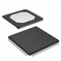
XC3S200-4TQG144I Xilinx Inc, XC3S200-4TQG144I Datasheet - Page 26

XC3S200-4TQG144I
Manufacturer Part Number
XC3S200-4TQG144I
Description
FPGA Spartan®-3 Family 200K Gates 4320 Cells 630MHz 90nm Technology 1.2V 144-Pin TQFP
Manufacturer
Xilinx Inc
Series
Spartan™-3r
Datasheet
1.XC3S50-4VQG100C.pdf
(217 pages)
Specifications of XC3S200-4TQG144I
Package
144TQFP
Family Name
Spartan®-3
Device Logic Units
4320
Device System Gates
200000
Maximum Internal Frequency
630 MHz
Typical Operating Supply Voltage
1.2 V
Maximum Number Of User I/os
97
Ram Bits
221184
Package / Case
144-TQFP, 144-VQFP
Mounting Type
Surface Mount
Voltage - Supply
1.14 V ~ 3.465 V
Operating Temperature
-40°C ~ 100°C
Number Of I /o
97
Number Of Logic Elements/cells
*
Number Of Gates
*
Lead Free Status / RoHS Status
Lead free / RoHS Compliant
Available stocks
Company
Part Number
Manufacturer
Quantity
Price
Company:
Part Number:
XC3S200-4TQG144I
Manufacturer:
XILINX
Quantity:
1 029
- Current page: 26 of 217
- Download datasheet (6Mb)
Spartan-3 FPGA Family: Functional Description
Table 12: Block RAM Port Signals
26
54
Address Bus
Data Input Bus
Parity Data
Input(s)
Description
Notes:
1.
2.
3.
4.
Signal
ADDRA[r
ADDRB[r
w
p
r
The control signals CLK, WE, EN, and SSR on both ports have the option of inverted polarity.
DIA[w
DIB[w
A
A
A
and r
DIPB[3:0]
and p
DIPA[3:0]
and w
SSRA
A
A
SSRB
B
B
CLKA
CLKB
WEA
WEB
–1:0]
–1:0]
–1:0]
–1:0]
B
ENA
ENB
B
B
are integers representing the address bus width at ports A and B, respectively.
are integers that indicate the number of data path lines serving as parity bits.
are integers representing the total data path width (i.e., data bits plus parity bits) at ports A and B, respectively.
ADDRA
Port A
Signal
Name
DIPA
DIA
RAMB16_Sw
(a) Dual-Port
ADDRB
Port B
Signal
Name
DIPB
DIB
A
_Sw
B
Figure 12: Block RAM Primitives
DOPA[p
DOA[w
DOPB[p
DOB[w
Direction
Input
Input
Input
A
B
A
–1:0]
B
–1:0]
–1:0]
–1:0]
www.xilinx.com
The Address Bus selects a memory location for read or write
operations. The width (w) of the port’s associated data path
determines the number of available address lines (r).
Whenever a port is enabled (ENA or ENB = High), address
transitions must meet the data sheet setup and hold times with
respect to the port clock (CLKA or CLKB). This requirement
must be met, even if the RAM read output is of no interest.
Data at the DI input bus is written to the addressed memory
location addressed on an enabled active CLK edge.
It is possible to configure a port’s total data path width (w) to be
1, 2, 4, 9, 18, or 36 bits. This selection applies to both the DI and
DO paths of a given port. Each port is independent. For a port
assigned a width (w), the number of addressable locations is
16,384/(w-p) where "p" is the number of parity bits. Each
memory location has a width of "w" (including parity bits). See
the DIP signal description for more information of parity.
Parity inputs represent additional bits included in the data input
path to support error detection. The number of parity bits "p"
included in the DI (same as for the DO bus) depends on a port’s
total data path width (w). See
ADDR[r–1:0]
DIP[p–1:0]
DI[w–1:0]
SSR
CLK
WE
EN
Function
(b) Single-Port
RAMB16_Sw
Table
DS099-2 (v2.5) December 4, 2009
13.
Product Specification
DOP[p–1:0]
DO[w–1:0]
DS099-2_13_112905
R
Related parts for XC3S200-4TQG144I
Image
Part Number
Description
Manufacturer
Datasheet
Request
R

Part Number:
Description:
IC SPARTAN-3 FPGA 200K 208-PQFP
Manufacturer:
Xilinx Inc
Datasheet:

Part Number:
Description:
IC SPARTAN-3 FPGA 200K 144-TQFP
Manufacturer:
Xilinx Inc
Datasheet:

Part Number:
Description:
SPARTAN-3A FPGA 200K STD 100VQFP
Manufacturer:
Xilinx Inc
Datasheet:

Part Number:
Description:
SPARTAN-3A FPGA 200K STD 100VQFP
Manufacturer:
Xilinx Inc

Part Number:
Description:
SPARTAN-3A FPGA 200K 144-TQFP
Manufacturer:
Xilinx Inc
Datasheet:

Part Number:
Description:
SPARTAN3A FPGA 200K STD 256FTBGA
Manufacturer:
Xilinx Inc
Datasheet:

Part Number:
Description:
IC FPGA SPARTAN 3 144TQFP
Manufacturer:
Xilinx Inc
Datasheet:

Part Number:
Description:
FLASH PROMS
Manufacturer:
Xilinx Inc
Datasheet:

Part Number:
Description:
FIELD PROGRAMMABLE G A
Manufacturer:
Xilinx Inc
Datasheet:

Part Number:
Description:
FPGA Spartan®-3 Family 200K Gates 4320 Cells 630MHz 90nm Technology 1.2V 256-Pin FTBGA
Manufacturer:
Xilinx Inc
Datasheet:

Part Number:
Description:
FPGA Spartan®-3 Family 200K Gates 4320 Cells 630MHz 90nm Technology 1.2V 256-Pin FTBGA
Manufacturer:
Xilinx Inc
Datasheet:

Part Number:
Description:
FPGA Spartan®-3 Family 200K Gates 4320 Cells 630MHz 90nm Technology 1.2V 208-Pin PQFP
Manufacturer:
Xilinx Inc
Datasheet:

Part Number:
Description:
FPGA Spartan®-3 Family 200K Gates 4320 Cells 630MHz 90nm Technology 1.2V 208-Pin PQFP
Manufacturer:
Xilinx Inc
Datasheet:

Part Number:
Description:
FPGA Spartan®-3 Family 200K Gates 4320 Cells 630MHz 90nm Technology 1.2V 144-Pin TQFP
Manufacturer:
Xilinx Inc
Datasheet:

Part Number:
Description:
FPGA Spartan®-3 Family 200K Gates 4320 Cells 630MHz 90nm Technology 1.2V 100-Pin VTQFP
Manufacturer:
Xilinx Inc
Datasheet:


