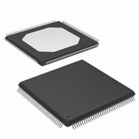
XC3S200-4TQG144I Xilinx Inc, XC3S200-4TQG144I Datasheet - Page 114

XC3S200-4TQG144I
Manufacturer Part Number
XC3S200-4TQG144I
Description
FPGA Spartan®-3 Family 200K Gates 4320 Cells 630MHz 90nm Technology 1.2V 144-Pin TQFP
Manufacturer
Xilinx Inc
Series
Spartan™-3r
Datasheet
1.XC3S50-4VQG100C.pdf
(217 pages)
Specifications of XC3S200-4TQG144I
Package
144TQFP
Family Name
Spartan®-3
Device Logic Units
4320
Device System Gates
200000
Maximum Internal Frequency
630 MHz
Typical Operating Supply Voltage
1.2 V
Maximum Number Of User I/os
97
Ram Bits
221184
Package / Case
144-TQFP, 144-VQFP
Mounting Type
Surface Mount
Voltage - Supply
1.14 V ~ 3.465 V
Operating Temperature
-40°C ~ 100°C
Number Of I /o
97
Number Of Logic Elements/cells
*
Number Of Gates
*
Lead Free Status / RoHS Status
Lead free / RoHS Compliant
Available stocks
Company
Part Number
Manufacturer
Quantity
Price
Company:
Part Number:
XC3S200-4TQG144I
Manufacturer:
XILINX
Quantity:
1 029
Spartan-3 FPGA Family: Pinout Descriptions
VCCAUX Type: Voltage Supply for Auxiliary
Logic
The VCCAUX pins supply power to various auxiliary cir-
cuits, such as to the Digital Clock Managers (DCMs), the
JTAG pins, and to the dedicated configuration pins (CON-
FIG type). VCCAUX must be +2.5V.
All VCCAUX inputs must be connected together and to the
+2.5V voltage supply. Furthermore, there must be sufficient
supply decoupling to guarantee problem-free operation, as
described in
Design: Using Bypass/Decoupling Capacitors
Because VCCAUX connects to the DCMs and the DCMs
are sensitive to voltage changes, be sure that the VCCAUX
supply and the ground return paths are designed for low
noise and low voltage drop, especially that caused by a
large number of simultaneous switching I/Os.
GND Type: Ground
All GND pins must be connected and have a low resistance
path back to the various VCCO, VCCINT, and VCCAUX
supplies.
Pin Behavior During Configuration
Table 78
configuration process. The actual behavior depends on the
values applied to the M2, M1, and M0 mode select pins and
the HSWAP_EN pin. The mode select pins determine which
of the DUAL type pins are active during configuration. In
Table 78: Pin Behavior After Power-Up, During Configuration
114
I/O: General-purpose I/O pins
IO
IO_Lxxy_#
DUAL: Dual-purpose configuration pins
IO_Lxxy_#/
DIN/D0
IO_Lxxy_#/
D1
IO_Lxxy_#/
D2
IO_Lxxy_#/
D3
IO_Lxxy_#/
D4
Pin Name
shows how various pins behave during the FPGA
XAPP623: Power Distribution System (PDS)
<0:0:0>
Master
DIN (I)
Serial Modes
Configuration Mode Settings <M2:M1:M0>
<1:1:1>
DIN (I)
Slave
.
www.xilinx.com
SelectMap Parallel Modes
D0 (I/O)
D1 (I/O)
D2 (I/O)
D3 (I/O)
D4 (I/O)
<0:1:1>
Master
JTAG configuration mode, none of the DUAL-type pins are
used for configuration and all behave as user-I/O pins.
All DUAL-type pins not actively used during configuration
and all I/O-type, DCI-type, VREF-type, GCLK-type pins are
high impedance (floating, three-stated, Hi-Z) during the
configuration process. These pins are indicated in
as shaded table entries or cells. These pins have a pull-up
resistor to their associated VCCO if the HSWAP_EN pin is
Low. When HSWAP_EN is High, these pull-up resistors are
disabled during configuration.
Some pins always have an active pull-up resistor during
configuration, regardless of the value applied to the
HSWAP_EN pin. After configuration, these pull-up resistors
are controlled by
•
•
•
After configuration completes, some pins have optional
behavior controlled by the configuration bitstream loaded
into the part. For example, via the bitstream, all unused I/O
pins can be collectively configured as input pins with either
a pull-up resistor, a pull-down resistor, or be left in a
high-impedance state.
All the dedicated CONFIG-type configuration pins
(CCLK,
HSWAP_EN) have a pull-up resistor to VCCAUX.
All JTAG-type pins (TCK, TDI, TMS, TDO) have a
pull-up resistor to VCCAUX.
The INIT_B DUAL-purpose pin has a pull-up resistor to
VCCO_4 or VCCO_BOTTOM, depending on package
style.
D0 (I/O)
D1 (I/O)
D2 (I/O)
D3 (I/O)
D4 (I/O)
<1:1:0>
Slave
PROG_B,
Bitstream
JTAG Mode
DONE,
<1:0:1>
DS099-4 (v2.5) December 4, 2009
Options.
M2,
Product Specification
Configuration
M1,
UnusedPin
UnusedPin
UnusedPin
UnusedPin
UnusedPin
UnusedPin
UnusedPin
Bitstream
Option
Persist
Persist
Persist
Persist
Persist
M0,
Table 78
and
R


