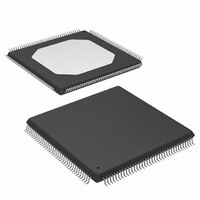
XC3S200-4TQG144I Xilinx Inc, XC3S200-4TQG144I Datasheet - Page 47

XC3S200-4TQG144I
Manufacturer Part Number
XC3S200-4TQG144I
Description
FPGA Spartan®-3 Family 200K Gates 4320 Cells 630MHz 90nm Technology 1.2V 144-Pin TQFP
Manufacturer
Xilinx Inc
Series
Spartan™-3r
Datasheet
1.XC3S50-4VQG100C.pdf
(217 pages)
Specifications of XC3S200-4TQG144I
Package
144TQFP
Family Name
Spartan®-3
Device Logic Units
4320
Device System Gates
200000
Maximum Internal Frequency
630 MHz
Typical Operating Supply Voltage
1.2 V
Maximum Number Of User I/os
97
Ram Bits
221184
Package / Case
144-TQFP, 144-VQFP
Mounting Type
Surface Mount
Voltage - Supply
1.14 V ~ 3.465 V
Operating Temperature
-40°C ~ 100°C
Number Of I /o
97
Number Of Logic Elements/cells
*
Number Of Gates
*
Lead Free Status / RoHS Status
Lead free / RoHS Compliant
Available stocks
Company
Part Number
Manufacturer
Quantity
Price
Company:
Part Number:
XC3S200-4TQG144I
Manufacturer:
XILINX
Quantity:
1 029
Slave Serial mode is selected by applying <111> to the
mode pins (M0, M1, and M2). A pull-up on the mode pins
makes slave serial the default mode if the pins are left
unconnected.
Master Serial Mode
In Master Serial mode, the FPGA drives CCLK pin, which
behaves as a bidirectional I/O pin. The FPGA in the center
of
the serial configuration PROM and to the CCLK inputs of
any slave FPGAs in a configuration daisy-chain. The master
FPGA drives the configuration clock on the CCLK pin to the
Xilinx Serial PROM, which, in response, provides bit-serial
data to the FPGA’s DIN input. The FPGA accepts this data
on each rising CCLK edge. After the master FPGA finishes
configuring, it passes data on its DOUT pin to the next
FPGA device in a daisy-chain. The DOUT data appears
after the falling CCLK clock edge.
The Master Serial mode interface is identical to Slave Serial
except that an internal oscillator generates the configuration
clock (CCLK). A wide range of frequencies can be selected
for CCLK, which always starts at a default frequency of
DS099-2 (v2.5) December 4, 2009
Product Specification
Figure 24
Notes:
1.
2.
R
is set for Master Serial mode and connects to
There are two ways to use the DONE line. First, one may set the BitGen option DriveDone to "Yes" only for the
last FPGA to be configured in the chain shown above (or for the single FPGA as may be the case). This enables
the DONE pin to drive High; thus, no pull-up resistor is necessary. DriveDone is set to "No" for the remaining
FPGAs in the chain. Second, DriveDone can be set to "No" for all FPGAs. Then all DONE lines are open-drain
and require the pull-up resistor shown in grey. In most cases, a value between 3.3KΩ to 4.7KΩ is sufficient.
However, when using DONE synchronously with a long chain of FPGAs, cumulative capacitance may
necessitate lower resistor values (e.g. down to 330Ω) in order to ensure a rise time within one clock cycle.
For information on how to program the FPGA using 3.3V signals and power, see
Interface.
3.3V: XCF0xS
1.8V: XCFxxP
Figure 24: Connection Diagram for Master and Slave Serial Configuration
V
CCINT
Flash PROM
Platform
XCF0xS
XCFxxP
GND
V
or
CCO
OE/RESET
V
CLK
CCJ
CE
CF
D0
2.5V
4.7KΩ
All
2.5V
2.5V
www.xilinx.com
DONE
INIT_B
PROG_B
CCLK
V
DIN
CCAUX
V
Spartan-3
CCO
Master
FPGA
GND
Bank 4
6 MHz. Configuration bits then switch CCLK to a higher fre-
quency for the remainder of the configuration.
Slave Parallel Mode (SelectMAP)
The Parallel or SelectMAP modes support the fastest con-
figuration. Byte-wide data is written into the FPGA with a
BUSY flag controlling the flow of data. An external source
provides 8-bit-wide data, CCLK, an active-Low Chip Select
(CS_B) signal and an active-Low Write signal (RDWR_B). If
BUSY is asserted (High) by the FPGA, the data must be
held until BUSY goes Low. Data can also be read using the
Slave Parallel mode. If RDWR_B is asserted, configuration
data is read out of the FPGA as part of a readback opera-
tion.
After configuration, it is possible to use any of the Multipur-
pose pins (DIN/D0-D7, DOUT/BUSY, INIT_B, CS_B, and
RDWR_B) as User I/Os. To do this, simply set the BitGen
option Persist to No and assign the desired signals to multi-
purpose configuration pins using the Xilinx development
software. Alternatively, it is possible to continue using the
configuration port (e.g. all configuration pins taken together)
V
DOUT
CCINT
M0
M1
M2
Spartan-3 FPGA Family: Functional Description
1.2V
2.5V
DONE
INIT_B
PROG_B
CCLK
V
DIN
3.3V-Tolerant Configuration
CCAUX
V
Spartan-3
CCO
FPGA
Slave
GND
Bank 4
DS099_23_112905
V
CCINT
M0
M1
M2
1.2V
2.5V
47


