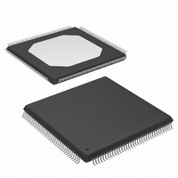
XC3S200-4TQG144I Xilinx Inc, XC3S200-4TQG144I Datasheet - Page 99

XC3S200-4TQG144I
Manufacturer Part Number
XC3S200-4TQG144I
Description
FPGA Spartan®-3 Family 200K Gates 4320 Cells 630MHz 90nm Technology 1.2V 144-Pin TQFP
Manufacturer
Xilinx Inc
Series
Spartan™-3r
Datasheet
1.XC3S50-4VQG100C.pdf
(217 pages)
Specifications of XC3S200-4TQG144I
Package
144TQFP
Family Name
Spartan®-3
Device Logic Units
4320
Device System Gates
200000
Maximum Internal Frequency
630 MHz
Typical Operating Supply Voltage
1.2 V
Maximum Number Of User I/os
97
Ram Bits
221184
Package / Case
144-TQFP, 144-VQFP
Mounting Type
Surface Mount
Voltage - Supply
1.14 V ~ 3.465 V
Operating Temperature
-40°C ~ 100°C
Number Of I /o
97
Number Of Logic Elements/cells
*
Number Of Gates
*
Lead Free Status / RoHS Status
Lead free / RoHS Compliant
Available stocks
Company
Part Number
Manufacturer
Quantity
Price
Company:
Part Number:
XC3S200-4TQG144I
Manufacturer:
XILINX
Quantity:
1 029
DS099-4 (v2.5) December 4, 2009
Introduction
This data sheet module describes the various pins on a
Spartan
component packages.
•
•
•
•
Table 68: Types of Pins on Spartan-3 FPGAs
© 2003–2009 Xilinx, Inc. XILINX, the Xilinx logo, Virtex, Spartan, ISE, and other designated brands included herein are trademarks of Xilinx in the United States and other coun-
tries. All other trademarks are the property of their respective owners.
DS099-4 (v2.5) December 4, 2009
Product Specification
CONFIG
DUAL
Type/
Color
Code
JTAG
The
pins by their function type.
The
description for each pin on the device.
The
offers significantly more detail about each pin,
especially for the dual- or special-function pins used
during device configuration.
Some pins have associated behavior that is controlled
by settings in the configuration bitstream. These
options are described in the
section.
DCI
I/O
®
-3 FPGA and how they connect to the supported
Pin Types
Detailed, Functional Pin Descriptions
Pin Definitions
Unrestricted, general-purpose user-I/O pin. Most pins can be paired
together to form differential I/Os.
Dual-purpose pin used in some configuration modes during the
configuration process and then usually available as a user I/O after
configuration. If the pin is not used during configuration, this pin behaves
as an I/O-type pin. There are 12 dual-purpose configuration pins on every
package. The INIT_B pin has an internal pull-up resistor to VCCO_4 or
VCCO_BOTTOM during configuration.
Dedicated configuration pin. Not available as a user-I/O pin. Every
package has seven dedicated configuration pins. These pins are powered
by VCCAUX and have a dedicated internal pull-up resistor to VCCAUX
during configuration.
Dedicated JTAG pin. Not available as a user-I/O pin. Every package has
four dedicated JTAG pins. These pins are powered by VCCAUX and have
a dedicated internal pull-up resistor to VCCAUX during configuration.
Dual-purpose pin that is either a user-I/O pin or used to calibrate output
buffer impedance for a specific bank using Digital Controlled Impedance
(DCI). There are two DCI pins per I/O bank.
section categorizes all of the FPGA
section provides a top-level
R
Bitstream Options
Description
section
217
www.xilinx.com
0
Spartan-3 FPGA Family:
Pinout Descriptions
Product Specification
•
Pin Descriptions
Pin Types
A majority of the pins on a Spartan-3 FPGA are gen-
eral-purpose, user-defined I/O pins. There are, however, up
to 12 different functional types of pins on Spartan-3 device
packages, as outlined in
drawings that follow, the individual pins are color-coded
according to pin type as in the table.
The
packaging options available for Spartan-3 FPGAs.
Detailed pin list tables and footprint diagrams are
provided for each package solution.
Package Overview
Table
IO,
IO_Lxxy_#
IO_Lxxy_#/DIN/D0,
IO_Lxxy_#/D1, IO_Lxxy_#/D2,
IO_Lxxy_#/D3, IO_Lxxy_#/D4,
IO_Lxxy_#/D5, IO_Lxxy_#/D6,
IO_Lxxy_#/D7,
IO_Lxxy_#/CS_B,
IO_Lxxy_#/RDWR_B,
IO_Lxxy_#/BUSY/DOUT,
IO_Lxxy_#/INIT_B
CCLK, DONE, M2, M1, M0,
PROG_B, HSWAP_EN
TDI, TMS, TCK, TDO
IO/VRN_#
IO_Lxxy_#/VRN_#
IO/VRP_#
IO_Lxxy_#/VRP_#
section describes the various
68. In the package footprint
Pin Name(s) in Type
99


