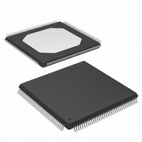
XC3S200-4TQG144I Xilinx Inc, XC3S200-4TQG144I Datasheet - Page 71

XC3S200-4TQG144I
Manufacturer Part Number
XC3S200-4TQG144I
Description
FPGA Spartan®-3 Family 200K Gates 4320 Cells 630MHz 90nm Technology 1.2V 144-Pin TQFP
Manufacturer
Xilinx Inc
Series
Spartan™-3r
Datasheet
1.XC3S50-4VQG100C.pdf
(217 pages)
Specifications of XC3S200-4TQG144I
Package
144TQFP
Family Name
Spartan®-3
Device Logic Units
4320
Device System Gates
200000
Maximum Internal Frequency
630 MHz
Typical Operating Supply Voltage
1.2 V
Maximum Number Of User I/os
97
Ram Bits
221184
Package / Case
144-TQFP, 144-VQFP
Mounting Type
Surface Mount
Voltage - Supply
1.14 V ~ 3.465 V
Operating Temperature
-40°C ~ 100°C
Number Of I /o
97
Number Of Logic Elements/cells
*
Number Of Gates
*
Lead Free Status / RoHS Status
Lead free / RoHS Compliant
Available stocks
Company
Part Number
Manufacturer
Quantity
Price
Company:
Part Number:
XC3S200-4TQG144I
Manufacturer:
XILINX
Quantity:
1 029
- Current page: 71 of 217
- Download datasheet (6Mb)
Table 43: Input Timing Adjustments for IOB
DS099-3 (v2.5) December 4, 2009
Product Specification
98
Following Signal Standard
Single-Ended Standards
GTL, GTL_DCI
GTLP, GTLP_DCI
HSLVDCI_15
HSLVDCI_18
HSLVDCI_25
HSLVDCI_33
HSTL_I, HSTL_I_DCI
HSTL_III, HSTL_III_DCI
HSTL_I_18,
HSTL_I_DCI_18
HSTL_II_18,
HSTL_II_DCI_18
HSTL_III_18,
HSTL_III_DCI_18
LVCMOS12
LVCMOS15
LVDCI_15
LVDCI_DV2_15
LVCMOS18
LVDCI_18
LVDCI_DV2_18
LVCMOS25
LVDCI_25
Convert Input Time from
LVCMOS25 to the
(IOSTANDARD)
R
Adjustment Below
0.44
0.36
0.51
0.29
0.51
0.51
0.51
0.37
0.36
0.39
0.45
0.63
0.42
0.38
0.38
0.24
0.29
0.28
0.05
Speed Grade
-5
0
Add the
0.50
0.42
0.59
0.33
0.59
0.59
0.59
0.42
0.41
0.45
0.52
0.72
0.49
0.43
0.44
0.28
0.33
0.33
0.05
-4
0
Spartan-3 FPGA Family: DC and Switching Characteristics
Units
ns
ns
ns
ns
ns
ns
ns
ns
ns
ns
ns
ns
ns
ns
ns
ns
ns
ns
ns
ns
www.xilinx.com
Table 43: Input Timing Adjustments for IOB (Continued)
Notes:
1.
2.
Following Signal Standard
LVDCI_DV2_25
LVCMOS33, LVDCI_33,
LVDCI_DV2_33
LVTTL
PCI33_3
SSTL18_I, SSTL18_I_DCI
SSTL18_II
SSTL2_I, SSTL2_I_DCI
SSTL2_II, SSTL2_II_DCI
Differential Standards
LDT_25 (ULVDS_25)
LVDS_25, LVDS_25_DCI
BLVDS_25
LVDSEXT_25,
LVDSEXT_25_DCI
LVPECL_25
RSDS_25
DIFF_HSTL_II_18,
DIFF_HSTL_II_18_DCI
DIFF_SSTL2_II
DIFF_SSTL2_II_DCI
Convert Input Time from
The numbers in this table are tested using the methodology
presented in
conditions set forth in
These adjustments are used to convert input path times
originally specified for the LVCMOS25 standard to times that
correspond to other signal standards.
LVCMOS25 to the
(IOSTANDARD)
Table 47
Table
and are based on the operating
Adjustment Below
31,
–0.05
0.04
0.18
0.20
0.39
0.39
0.40
0.36
0.76
0.65
0.34
0.80
0.18
0.43
0.34
0.65
Speed Grade
-5
Table
Add the
34, and
–0.02
0.04
0.21
0.22
0.45
0.45
0.46
0.41
0.88
0.75
0.39
0.92
0.21
0.50
0.39
0.75
-4
Table
36.
Units
ns
ns
ns
ns
ns
ns
ns
ns
ns
ns
ns
ns
ns
ns
ns
ns
71
Related parts for XC3S200-4TQG144I
Image
Part Number
Description
Manufacturer
Datasheet
Request
R

Part Number:
Description:
IC SPARTAN-3 FPGA 200K 208-PQFP
Manufacturer:
Xilinx Inc
Datasheet:

Part Number:
Description:
IC SPARTAN-3 FPGA 200K 144-TQFP
Manufacturer:
Xilinx Inc
Datasheet:

Part Number:
Description:
SPARTAN-3A FPGA 200K STD 100VQFP
Manufacturer:
Xilinx Inc
Datasheet:

Part Number:
Description:
SPARTAN-3A FPGA 200K STD 100VQFP
Manufacturer:
Xilinx Inc

Part Number:
Description:
SPARTAN-3A FPGA 200K 144-TQFP
Manufacturer:
Xilinx Inc
Datasheet:

Part Number:
Description:
SPARTAN3A FPGA 200K STD 256FTBGA
Manufacturer:
Xilinx Inc
Datasheet:

Part Number:
Description:
IC FPGA SPARTAN 3 144TQFP
Manufacturer:
Xilinx Inc
Datasheet:

Part Number:
Description:
FLASH PROMS
Manufacturer:
Xilinx Inc
Datasheet:

Part Number:
Description:
FIELD PROGRAMMABLE G A
Manufacturer:
Xilinx Inc
Datasheet:

Part Number:
Description:
FPGA Spartan®-3 Family 200K Gates 4320 Cells 630MHz 90nm Technology 1.2V 256-Pin FTBGA
Manufacturer:
Xilinx Inc
Datasheet:

Part Number:
Description:
FPGA Spartan®-3 Family 200K Gates 4320 Cells 630MHz 90nm Technology 1.2V 256-Pin FTBGA
Manufacturer:
Xilinx Inc
Datasheet:

Part Number:
Description:
FPGA Spartan®-3 Family 200K Gates 4320 Cells 630MHz 90nm Technology 1.2V 208-Pin PQFP
Manufacturer:
Xilinx Inc
Datasheet:

Part Number:
Description:
FPGA Spartan®-3 Family 200K Gates 4320 Cells 630MHz 90nm Technology 1.2V 208-Pin PQFP
Manufacturer:
Xilinx Inc
Datasheet:

Part Number:
Description:
FPGA Spartan®-3 Family 200K Gates 4320 Cells 630MHz 90nm Technology 1.2V 144-Pin TQFP
Manufacturer:
Xilinx Inc
Datasheet:

Part Number:
Description:
FPGA Spartan®-3 Family 200K Gates 4320 Cells 630MHz 90nm Technology 1.2V 100-Pin VTQFP
Manufacturer:
Xilinx Inc
Datasheet:


