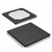
XC3S200-4TQG144I Xilinx Inc, XC3S200-4TQG144I Datasheet - Page 78

XC3S200-4TQG144I
Manufacturer Part Number
XC3S200-4TQG144I
Description
FPGA Spartan®-3 Family 200K Gates 4320 Cells 630MHz 90nm Technology 1.2V 144-Pin TQFP
Manufacturer
Xilinx Inc
Series
Spartan™-3r
Datasheet
1.XC3S50-4VQG100C.pdf
(217 pages)
Specifications of XC3S200-4TQG144I
Package
144TQFP
Family Name
Spartan®-3
Device Logic Units
4320
Device System Gates
200000
Maximum Internal Frequency
630 MHz
Typical Operating Supply Voltage
1.2 V
Maximum Number Of User I/os
97
Ram Bits
221184
Package / Case
144-TQFP, 144-VQFP
Mounting Type
Surface Mount
Voltage - Supply
1.14 V ~ 3.465 V
Operating Temperature
-40°C ~ 100°C
Number Of I /o
97
Number Of Logic Elements/cells
*
Number Of Gates
*
Lead Free Status / RoHS Status
Lead free / RoHS Compliant
Available stocks
Company
Part Number
Manufacturer
Quantity
Price
Company:
Part Number:
XC3S200-4TQG144I
Manufacturer:
XILINX
Quantity:
1 029
Spartan-3 FPGA Family: DC and Switching Characteristics
Table 47: Test Methods for Timing Measurement at I/Os (Continued)
The capacitive load (C
and GND. The Output timing for all standards, as published
in the speed files and the data sheet, is always based on a
C
are used for all measurements. Any delay that the test fix-
ture might contribute to test measurements is subtracted
from those measurements to produce the final timing num-
bers as published in the speed files and data sheet.
Using IBIS Models to Simulate Load
Conditions in Application
IBIS Models permit the most accurate prediction of timing
delays for a given application. The parameters found in the
IBIS model (V
with the parameters used in
not confuse V
model with V
table. A fourth parameter, C
parameters describe all relevant output test conditions. IBIS
78
Notes:
1.
2.
3.
DIFF_SSTL2_II
DIFF_SSTL2_II_DCI
L
value of zero. High-impedance probes (less than 1 pF)
Descriptions of the relevant symbols are as follows:
The load capacitance (C
According to the PCI specification.
Signal Standard
(IOSTANDARD)
V
V
V
V
V
R
V
REF
ICM
M
L
H
T
T
–
–
–
–
–
–
Low-level test voltage at Input pin
Effective termination resistance, which takes on a value of 1M
Termination voltage
–
High-level test voltage at Input pin
REF
Voltage of measurement point on signal transition
REF
REF
The common mode input voltage
The reference voltage for setting the input switching threshold
, R
(the input-switching threshold) from the
(the termination voltage) from the IBIS
REF
L
) is connected between the output
, and V
L
) at the Output pin is 0 pF for all signal standards.
REF
Table
V
REF
, is always zero. The four
MEAS
-
(V)
47, V
) correspond directly
T
, R
V
T
ICM
, and V
V
Inputs
L
- 0.75
(V)
M
www.xilinx.com
. Do
V
ICM
V
models are found in the Xilinx development software as well
as at the following link.
Simulate delays for a given application according to its spe-
cific load conditions as follows:
1. Simulate the desired signal standard with the output
2. Record the time to V
3. Simulate the same signal standard with the output
4. Record the time to V
5. Compare the results of steps 2 and 4. The increase (or
H
+ 0.75
(V)
http://www.xilinx.com/support/download/index.htm
driver connected to the test setup shown in
Use parameter values V
C
driver connected to the PCB trace with load. Use the
appropriate IBIS model (including V
and V
load.
decrease) in delay should be added to (or subtracted
from) the appropriate Output standard adjustment
REF
Ω
when no parallel termination is required
is zero.
MEAS
R
values) or capacitive value to represent the
T
50
(Ω)
Outputs
M
MEAS
.
DS099-3 (v2.5) December 4, 2009
T
, R
.
V
T
1.25
, and V
T
(V)
Product Specification
REF
M
from
, R
Inputs and
REF
Outputs
Table
Figure
V
V
M
, C
ICM
(V)
REF
47.
33.
,
R


