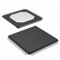
XC3S200-4TQG144I Xilinx Inc, XC3S200-4TQG144I Datasheet - Page 162

XC3S200-4TQG144I
Manufacturer Part Number
XC3S200-4TQG144I
Description
FPGA Spartan®-3 Family 200K Gates 4320 Cells 630MHz 90nm Technology 1.2V 144-Pin TQFP
Manufacturer
Xilinx Inc
Series
Spartan™-3r
Datasheet
1.XC3S50-4VQG100C.pdf
(217 pages)
Specifications of XC3S200-4TQG144I
Package
144TQFP
Family Name
Spartan®-3
Device Logic Units
4320
Device System Gates
200000
Maximum Internal Frequency
630 MHz
Typical Operating Supply Voltage
1.2 V
Maximum Number Of User I/os
97
Ram Bits
221184
Package / Case
144-TQFP, 144-VQFP
Mounting Type
Surface Mount
Voltage - Supply
1.14 V ~ 3.465 V
Operating Temperature
-40°C ~ 100°C
Number Of I /o
97
Number Of Logic Elements/cells
*
Number Of Gates
*
Lead Free Status / RoHS Status
Lead free / RoHS Compliant
Available stocks
Company
Part Number
Manufacturer
Quantity
Price
Company:
Part Number:
XC3S200-4TQG144I
Manufacturer:
XILINX
Quantity:
1 029
Spartan-3 FPGA Family: Pinout Descriptions
FG676: 676-lead Fine-pitch Ball Grid
Array
The 676-lead fine-pitch ball grid array package, FG676,
supports five different Spartan-3 devices, including the
XC3S1000, XC3S1500, XC3S2000, XC3S4000, and
XC3S5000. All five have nearly identical footprints but are
slightly different, primarily due to unconnected pins on the
XC3S1000 and XC3S1500. For example, because the
XC3S1000 has fewer I/O pins, this device has 98 uncon-
nected pins on the FG676 package, labeled as “N.C.” In
Table 102
cated with a black diamond symbol ( ). The XC3S1500,
however, has only two unconnected pins, also labeled
“N.C.” in the pinout table but indicated with a black square
symbol ( ).
All the package pins appear in
bank number, then by pin name. Pairs of pins that form a dif-
ferential I/O pair appear together in the table. The table also
shows the pin number for each pin and the pin type, as
defined earlier.
Pinout Table
Table 102: FG676 Package Pinout
162
Bank
0
0
0
0
0
0
0
0
0
0
0
0
0
0
0
0
0
0
0
0
0
0
0
0
0
0
IO
IO
IO
IO
N.C. ( )
IO
IO
IO
IO
IO/VREF_0
IO/VREF_0
IO/VREF_0
IO_L01N_0/VRP_0
IO_L01P_0/VRN_0
IO_L05N_0
IO_L05P_0/VREF_0
IO_L06N_0
IO_L06P_0
IO_L07N_0
IO_L07P_0
IO_L08N_0
IO_L08P_0
IO_L09N_0
IO_L09P_0
IO_L10N_0
IO_L10P_0
and
XC3S1000
Pin Name
Figure
49, these unconnected pins are indi-
IO
IO
IO
IO
IO
IO
IO
IO
IO
IO/VREF_0
IO/VREF_0
IO/VREF_0
IO_L01N_0/VRP_0
IO_L01P_0/VRN_0
IO_L05N_0
IO_L05P_0/VREF_0
IO_L06N_0
IO_L06P_0
IO_L07N_0
IO_L07P_0
IO_L08N_0
IO_L08P_0
IO_L09N_0
IO_L09P_0
IO_L10N_0
IO_L10P_0
XC3S1500
Pin Name
Table 102
and are sorted by
IO
IO
IO
IO
IO
IO
IO
IO
IO
IO/VREF_0
IO/VREF_0
IO/VREF_0
IO_L01N_0/VRP_0
IO_L01P_0/VRN_0
IO_L05N_0
IO_L05P_0/VREF_0
IO_L06N_0
IO_L06P_0
IO_L07N_0
IO_L07P_0
IO_L08N_0
IO_L08P_0
IO_L09N_0
IO_L09P_0
IO_L10N_0
IO_L10P_0
XC3S2000
Pin Name
www.xilinx.com
If there is a difference between the XC3S1000, XC3S1500,
XC3S2000, XC3S4000, and XC3S5000 pinouts, then that
difference is highlighted in
shaded grey, then there is an unconnected pin on either the
XC3S1000 or XC3S1500 that maps to a user-I/O pin on the
XC3S2000, XC3S4000, and XC3S5000. If the table entry is
shaded tan, then the unconnected pin on either the
XC3S1000 or XC3S1500 maps to a VREF-type pin on the
XC3S2000, XC3S4000, and XC3S5000. If the other VREF
pins in the bank all connect to a voltage reference to support
a special I/O standard, then also connect the N.C. pin on the
XC3S1000 or XC3S1500 to the same VREF voltage. This
provides maximum flexibility as you could potentially
migrate a design from the XC3S1000 through to the
XC3S5000 FPGA without changing the printed circuit
board.
An electronic version of this package pinout table and foot-
print diagram is available for download from the Xilinx web-
site at
sheets/s3_pin.zip
IO
IO
IO
IO
IO
IO
IO
IO
IO
IO/VREF_0
IO/VREF_0
IO/VREF_0
IO_L01N_0/VRP_0
IO_L01P_0/VRN_0
IO_L05N_0
IO_L05P_0/VREF_0
IO_L06N_0
IO_L06P_0
IO_L07N_0
IO_L07P_0
IO_L08N_0
IO_L08P_0
IO_L09N_0
IO_L09P_0
IO_L10N_0
IO_L10P_0
XC3S4000
Pin Name
http://www.xilinx.com/support/documentation/data_
.
IO_L04N_0
IO
IO
IO_L04P_0
IO_L13N_0
IO
IO
IO
IO
IO/VREF_0
IO/VREF_0
IO/VREF_0
IO_L01N_0/VRP_0
IO_L01P_0/VRN_0
IO_L05N_0
IO_L05P_0/VREF_0
IO_L06N_0
IO_L06P_0
IO_L07N_0
IO_L07P_0
IO_L08N_0
IO_L08P_0
IO_L09N_0
IO_L09P_0
IO_L10N_0
IO_L10P_0
XC3S5000
Pin Name
Table
DS099-4 (v2.5) December 4, 2009
3
3
3
102. If the table entry is
Product Specification
Pin Number
FG676
C12
H11
H12
G10
E13
A3
A5
A6
C4
C8
B3
E5
D5
B4
A4
C5
B5
E6
D6
C6
B6
E7
D7
B7
A7
F7
VREF
VREF
VREF
VREF
Type
DCI
DCI
I/O
I/O
I/O
I/O
I/O
I/O
I/O
I/O
I/O
I/O
I/O
I/O
I/O
I/O
I/O
I/O
I/O
I/O
I/O
I/O
R


