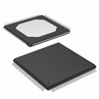
XC3S200-4TQG144I Xilinx Inc, XC3S200-4TQG144I Datasheet - Page 22

XC3S200-4TQG144I
Manufacturer Part Number
XC3S200-4TQG144I
Description
FPGA Spartan®-3 Family 200K Gates 4320 Cells 630MHz 90nm Technology 1.2V 144-Pin TQFP
Manufacturer
Xilinx Inc
Series
Spartan™-3r
Datasheet
1.XC3S50-4VQG100C.pdf
(217 pages)
Specifications of XC3S200-4TQG144I
Package
144TQFP
Family Name
Spartan®-3
Device Logic Units
4320
Device System Gates
200000
Maximum Internal Frequency
630 MHz
Typical Operating Supply Voltage
1.2 V
Maximum Number Of User I/os
97
Ram Bits
221184
Package / Case
144-TQFP, 144-VQFP
Mounting Type
Surface Mount
Voltage - Supply
1.14 V ~ 3.465 V
Operating Temperature
-40°C ~ 100°C
Number Of I /o
97
Number Of Logic Elements/cells
*
Number Of Gates
*
Lead Free Status / RoHS Status
Lead free / RoHS Compliant
Available stocks
Company
Part Number
Manufacturer
Quantity
Price
Company:
Part Number:
XC3S200-4TQG144I
Manufacturer:
XILINX
Quantity:
1 029
Spartan-3 FPGA Family: Functional Description
.
CLB Overview
For more details on the CLBs, refer to the “Using Config-
urable Logic Blocks” chapter in UG331.
The Configurable Logic Blocks (CLBs) constitute the main
logic resource for implementing synchronous as well as
combinatorial circuits. Each CLB comprises four intercon-
nected slices, as shown in
grouped in pairs. Each pair is organized as a column with an
independent carry chain.
The nomenclature that the FPGA Editor — part of the Xilinx
development software — uses to designate slices is as fol-
lows: The letter ‘X’ followed by a number identifies columns
of slices. The ‘X’ number counts up in sequence from the
left side of the die to the right. The letter ‘Y’ followed by a
number identifies the position of each slice in a pair as well
as indicating the CLB row. The ‘Y’ number counts slices
starting from the bottom of the die according to the
sequence: 0, 1, 0, 1 (the first CLB row); 2, 3, 2, 3 (the sec-
ond CLB row); etc.
lower left-hand corner of the die. Slices X0Y0 and X0Y1
make up the column-pair on the left where as slices X1Y0
and X1Y1 make up the column-pair on the right. For each
CLB, the term “left-hand” (or SLICEM) indicates the pair of
slices labeled with an even ‘X’ number, such as X0, and the
term “right-hand” (or SLICEL) designates the pair of slices
with an odd ‘X’ number, e.g., X1.
Elements Within a Slice
All four slices have the following elements in common: two
logic function generators, two storage elements, wide-func-
tion multiplexers, carry logic, and arithmetic gates, as
22
54
Figure 9
Switch
Matrix
shows the CLB located in the
Figure
SHIFTOUT
SHIFTIN
(Logic or Distributed RAM
Figure 9: Arrangement of Slices within the CLB
9. These slices are
Left-Hand SLICEM
or Shift Register)
CLB
SLICE
SLICE
X0Y1
X0Y0
COUT
CIN
www.xilinx.com
shown in
pairs use these elements to provide logic, arithmetic, and
ROM functions. Besides these, the left-hand pair supports
two additional functions: storing data using Distributed RAM
and shifting data with 16-bit registers.
gram of the left-hand slice; therefore, it represents a super-
set of the elements and connections to be found in all slices.
See
The RAM-based function generator — also known as a
Look-Up Table or LUT — is the main resource for imple-
menting logic functions. Furthermore, the LUTs in each
left-hand slice pair can be configured as Distributed RAM or
a 16-bit shift register. For information on the former, refer to
the “Using Look-Up Tables as Distributed RAM” chapter in
UG331.; for information on the latter, refer to the “Using
Look-Up Tables as Shift Registers” chapter in UG331. The
function generators located in the upper and lower portions
of the slice are referred to as the "G" and "F", respectively.
The storage element, which is programmable as either a
D-type flip-flop or a level-sensitive latch, provides a means
for synchronizing data to a clock signal, among other uses.
The storage elements in the upper and lower portions of the
slice are called FFY and FFX, respectively.
Wide-function multiplexers effectively combine LUTs in
order to permit more complex logic operations. Each slice
has two of these multiplexers with F5MUX in the lower por-
tion of the slice and FiMUX in the upper portion. Depending
on the slice, FiMUX takes on the name F6MUX, F7MUX, or
F8MUX. For more details on the multiplexers, refer to the
“Using Dedicated Multiplexers” chapter in UG331.
Right-Hand SLICEL
(Logic Only)
Function Generator, page 24
SLICE
SLICE
X1Y1
X1Y0
COUT
CIN
Figure
10. Both the left-hand and right-hand slice
DS099-2_05_082104
to Neighbors
Interconnect
DS099-2 (v2.5) December 4, 2009
for more information.
Product Specification
Figure 10
is a dia-
R


