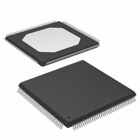
XC3S200-4TQG144I Xilinx Inc, XC3S200-4TQG144I Datasheet - Page 90

XC3S200-4TQG144I
Manufacturer Part Number
XC3S200-4TQG144I
Description
FPGA Spartan®-3 Family 200K Gates 4320 Cells 630MHz 90nm Technology 1.2V 144-Pin TQFP
Manufacturer
Xilinx Inc
Series
Spartan™-3r
Datasheet
1.XC3S50-4VQG100C.pdf
(217 pages)
Specifications of XC3S200-4TQG144I
Package
144TQFP
Family Name
Spartan®-3
Device Logic Units
4320
Device System Gates
200000
Maximum Internal Frequency
630 MHz
Typical Operating Supply Voltage
1.2 V
Maximum Number Of User I/os
97
Ram Bits
221184
Package / Case
144-TQFP, 144-VQFP
Mounting Type
Surface Mount
Voltage - Supply
1.14 V ~ 3.465 V
Operating Temperature
-40°C ~ 100°C
Number Of I /o
97
Number Of Logic Elements/cells
*
Number Of Gates
*
Lead Free Status / RoHS Status
Lead free / RoHS Compliant
Available stocks
Company
Part Number
Manufacturer
Quantity
Price
Company:
Part Number:
XC3S200-4TQG144I
Manufacturer:
XILINX
Quantity:
1 029
- Current page: 90 of 217
- Download datasheet (6Mb)
Spartan-3 FPGA Family: DC and Switching Characteristics
Phase Shifter (PS)
Phase shifter operation is only supported if the DLL is in low-frequency mode, see
software version 10.1.03 (or later).
Table 61: Recommended Operating Conditions for the PS in Variable Phase Mode
Table 62: Switching Characteristics for the PS in Variable or Fixed Phase Shift Mode
90
Notes:
1.
2.
Operating Frequency Ranges
PSCLK_FREQ
(F
Input Pulse Requirements
PSCLK_PULSE
Phase Shifting Range
FINE_SHIFT_RANGE
Lock Time
LOCK_DLL_PS
LOCK_DLL_PS_FX
PSCLK
The numbers in this table are based on the operating conditions set forth in
The PS specifications in this table apply when the PS attribute CLKOUT_PHASE_SHIFT= VARIABLE or FIXED.
Symbol
Symbol
)
Frequency for the
PSCLK input
PSCLK pulse width
as a percentage of
the PSCLK period
Description
Phase shift range
When using the PS in conjunction
with the DLL: The time from
deassertion at the DCM’s Reset
input to the rising transition at its
LOCKED output. When the DCM
is locked, the CLKIN and CLKFB
signals are in phase.
When using the PS in conjunction
with the DLL and DFS: The time
from deassertion at the DCM’s
Reset input to the rising transition
at its LOCKED output. When the
DCM is locked, the CLKIN and
CLKFB signals are in phase.
Description
Low
Frequency Mode/
F
CLKIN
F
F
Low
CLKIN
CLKIN
www.xilinx.com
Range
60 MHz < F
18 MHz < F
30 MHz < F
40 MHz < F
50 MHz < F
< 100 MHz
> 100 MHz
Frequency Mode/
F
CLKIN
CLKIN
Low
CLKIN
CLKIN
CLKIN
CLKIN
Low
Range
< 165 MHz
< 30 MHz
< 40 MHz
< 50 MHz
< 60 MHz
40%
45%
Table 31
Min
1
-5
and
Table
60%
55%
Max
167
Speed Grade
Table
Min
-
-
-
-
-
-
-
57. Fixed phase shift requires ISE
-5
61.
DS099-3 (v2.5) December 4, 2009
10.40
Speed Grade
Max
10.0
3.28
2.56
1.60
1.00
0.88
40%
45%
Min
1
-4
Min
Product Specification
-
-
-
-
-
-
-
60%
55%
Max
167
-4
10.40
Max
10.0
3.28
2.56
1.60
1.00
0.88
Units
MHz
Units
-
-
ms
ms
ms
ms
ms
ms
ns
R
Related parts for XC3S200-4TQG144I
Image
Part Number
Description
Manufacturer
Datasheet
Request
R

Part Number:
Description:
IC SPARTAN-3 FPGA 200K 208-PQFP
Manufacturer:
Xilinx Inc
Datasheet:

Part Number:
Description:
IC SPARTAN-3 FPGA 200K 144-TQFP
Manufacturer:
Xilinx Inc
Datasheet:

Part Number:
Description:
SPARTAN-3A FPGA 200K STD 100VQFP
Manufacturer:
Xilinx Inc
Datasheet:

Part Number:
Description:
SPARTAN-3A FPGA 200K STD 100VQFP
Manufacturer:
Xilinx Inc

Part Number:
Description:
SPARTAN-3A FPGA 200K 144-TQFP
Manufacturer:
Xilinx Inc
Datasheet:

Part Number:
Description:
SPARTAN3A FPGA 200K STD 256FTBGA
Manufacturer:
Xilinx Inc
Datasheet:

Part Number:
Description:
IC FPGA SPARTAN 3 144TQFP
Manufacturer:
Xilinx Inc
Datasheet:

Part Number:
Description:
FLASH PROMS
Manufacturer:
Xilinx Inc
Datasheet:

Part Number:
Description:
FIELD PROGRAMMABLE G A
Manufacturer:
Xilinx Inc
Datasheet:

Part Number:
Description:
FPGA Spartan®-3 Family 200K Gates 4320 Cells 630MHz 90nm Technology 1.2V 256-Pin FTBGA
Manufacturer:
Xilinx Inc
Datasheet:

Part Number:
Description:
FPGA Spartan®-3 Family 200K Gates 4320 Cells 630MHz 90nm Technology 1.2V 256-Pin FTBGA
Manufacturer:
Xilinx Inc
Datasheet:

Part Number:
Description:
FPGA Spartan®-3 Family 200K Gates 4320 Cells 630MHz 90nm Technology 1.2V 208-Pin PQFP
Manufacturer:
Xilinx Inc
Datasheet:

Part Number:
Description:
FPGA Spartan®-3 Family 200K Gates 4320 Cells 630MHz 90nm Technology 1.2V 208-Pin PQFP
Manufacturer:
Xilinx Inc
Datasheet:

Part Number:
Description:
FPGA Spartan®-3 Family 200K Gates 4320 Cells 630MHz 90nm Technology 1.2V 144-Pin TQFP
Manufacturer:
Xilinx Inc
Datasheet:

Part Number:
Description:
FPGA Spartan®-3 Family 200K Gates 4320 Cells 630MHz 90nm Technology 1.2V 100-Pin VTQFP
Manufacturer:
Xilinx Inc
Datasheet:


