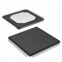
XC3S200-4TQG144I Xilinx Inc, XC3S200-4TQG144I Datasheet - Page 76

XC3S200-4TQG144I
Manufacturer Part Number
XC3S200-4TQG144I
Description
FPGA Spartan®-3 Family 200K Gates 4320 Cells 630MHz 90nm Technology 1.2V 144-Pin TQFP
Manufacturer
Xilinx Inc
Series
Spartan™-3r
Datasheet
1.XC3S50-4VQG100C.pdf
(217 pages)
Specifications of XC3S200-4TQG144I
Package
144TQFP
Family Name
Spartan®-3
Device Logic Units
4320
Device System Gates
200000
Maximum Internal Frequency
630 MHz
Typical Operating Supply Voltage
1.2 V
Maximum Number Of User I/os
97
Ram Bits
221184
Package / Case
144-TQFP, 144-VQFP
Mounting Type
Surface Mount
Voltage - Supply
1.14 V ~ 3.465 V
Operating Temperature
-40°C ~ 100°C
Number Of I /o
97
Number Of Logic Elements/cells
*
Number Of Gates
*
Lead Free Status / RoHS Status
Lead free / RoHS Compliant
Available stocks
Company
Part Number
Manufacturer
Quantity
Price
Company:
Part Number:
XC3S200-4TQG144I
Manufacturer:
XILINX
Quantity:
1 029
- Current page: 76 of 217
- Download datasheet (6Mb)
Spartan-3 FPGA Family: DC and Switching Characteristics
Timing Measurement Methodology
When measuring timing parameters at the programmable
I/Os, different signal standards call for different test condi-
tions.
dard.
The method for measuring Input timing is as follows: A sig-
nal that swings between a Low logic level of V
logic level of V
standards also require the application of a bias voltage to
the V
input-switching threshold. The measurement point of the
Input signal (V
and V
The Output test setup is shown in
voltage V
end of which is connected to the Output. For each standard,
R
mended for minimizing signal reflections. If the standard
does not ordinarily use terminations (e.g., LVCMOS,
Table 47: Test Methods for Timing Measurement at I/Os
76
Single-Ended
GTL
GTL_DCI
GTLP
GTLP_DCI
HSLVDCI_15
HSLVDCI_18
HSLVDCI_25
HSLVDCI_33
HSTL_I
HSTL_I_DCI
HSTL_III
HSTL_III_DCI
HSTL_I_18
HSTL_I_DCI_18
HSTL_II_18
HSTL_II_DCI_18
HSTL_III_18
HSTL_III_DCI_18
LVCMOS12
LVCMOS15
LVDCI_15
LVDCI_DV2_15
HSLVDCI_15
T
and V
Signal Standard
Table 47
H
(IOSTANDARD)
REF
.
T
T
is applied to the termination resistor R
pins of a given bank to properly set the
generally take on the standard values recom-
M
presents the conditions to use for each stan-
H
) is commonly located halfway between V
is applied to the Input under test. Some
V
REF
0.90
0.75
0.90
0.90
0.8
1.0
0.9
1.1
-
-
Figure
(V)
33. A termination
V
V
V
V
V
V
V
V
REF
REF
REF
REF
REF
REF
REF
REF
V
L
Inputs
L
and a High
0
0
T
(V)
, the other
- 0.2
- 0.2
- 0.5
- 0.5
- 0.5
- 0.5
- 0.5
- 0.5
www.xilinx.com
L
V
V
V
V
V
V
V
V
REF
REF
REF
REF
REF
REF
REF
REF
V
LVTTL), then R
tion, and V
(V
H
1.2
1.5
(V)
+ 0.2
+ 0.2
+ 0.5
+ 0.5
+ 0.5
+ 0.5
+ 0.5
+ 0.5
M
) that was used at the Input is also used at the Output.
Notes:
1.
FPGA Output
T
is set to zero. The same measurement point
Figure 33: Output Test Setup
The names shown in parentheses are
used in the IBIS file.
T
R
1M
1M
1M
T
is set to 1MΩ to indicate an open connec-
25
50
25
50
50
50
50
50
50
(Ω)
Outputs
V
T
(V
DS099-3 (v2.5) December 4, 2009
REF
R
C
T
L
V
0.75
(R
T
1.2
1.2
1.5
1.5
1.5
0.9
0.9
1.8
)
(C
V
0
0
0
(V)
M
REF
REF
(V
ds099-3_07_012004
Product Specification
)
MEAS
)
)
Inputs and
Outputs
V
V
V
V
V
V
V
V
0.75
0.90
1.25
1.65
0.75
M
0.6
REF
REF
REF
REF
REF
REF
REF
(V)
R
Related parts for XC3S200-4TQG144I
Image
Part Number
Description
Manufacturer
Datasheet
Request
R

Part Number:
Description:
IC SPARTAN-3 FPGA 200K 208-PQFP
Manufacturer:
Xilinx Inc
Datasheet:

Part Number:
Description:
IC SPARTAN-3 FPGA 200K 144-TQFP
Manufacturer:
Xilinx Inc
Datasheet:

Part Number:
Description:
SPARTAN-3A FPGA 200K STD 100VQFP
Manufacturer:
Xilinx Inc
Datasheet:

Part Number:
Description:
SPARTAN-3A FPGA 200K STD 100VQFP
Manufacturer:
Xilinx Inc

Part Number:
Description:
SPARTAN-3A FPGA 200K 144-TQFP
Manufacturer:
Xilinx Inc
Datasheet:

Part Number:
Description:
SPARTAN3A FPGA 200K STD 256FTBGA
Manufacturer:
Xilinx Inc
Datasheet:

Part Number:
Description:
IC FPGA SPARTAN 3 144TQFP
Manufacturer:
Xilinx Inc
Datasheet:

Part Number:
Description:
FLASH PROMS
Manufacturer:
Xilinx Inc
Datasheet:

Part Number:
Description:
FIELD PROGRAMMABLE G A
Manufacturer:
Xilinx Inc
Datasheet:

Part Number:
Description:
FPGA Spartan®-3 Family 200K Gates 4320 Cells 630MHz 90nm Technology 1.2V 256-Pin FTBGA
Manufacturer:
Xilinx Inc
Datasheet:

Part Number:
Description:
FPGA Spartan®-3 Family 200K Gates 4320 Cells 630MHz 90nm Technology 1.2V 256-Pin FTBGA
Manufacturer:
Xilinx Inc
Datasheet:

Part Number:
Description:
FPGA Spartan®-3 Family 200K Gates 4320 Cells 630MHz 90nm Technology 1.2V 208-Pin PQFP
Manufacturer:
Xilinx Inc
Datasheet:

Part Number:
Description:
FPGA Spartan®-3 Family 200K Gates 4320 Cells 630MHz 90nm Technology 1.2V 208-Pin PQFP
Manufacturer:
Xilinx Inc
Datasheet:

Part Number:
Description:
FPGA Spartan®-3 Family 200K Gates 4320 Cells 630MHz 90nm Technology 1.2V 144-Pin TQFP
Manufacturer:
Xilinx Inc
Datasheet:

Part Number:
Description:
FPGA Spartan®-3 Family 200K Gates 4320 Cells 630MHz 90nm Technology 1.2V 100-Pin VTQFP
Manufacturer:
Xilinx Inc
Datasheet:


