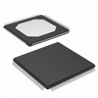
XC3S200-4TQG144I Xilinx Inc, XC3S200-4TQG144I Datasheet - Page 61

XC3S200-4TQG144I
Manufacturer Part Number
XC3S200-4TQG144I
Description
FPGA Spartan®-3 Family 200K Gates 4320 Cells 630MHz 90nm Technology 1.2V 144-Pin TQFP
Manufacturer
Xilinx Inc
Series
Spartan™-3r
Datasheet
1.XC3S50-4VQG100C.pdf
(217 pages)
Specifications of XC3S200-4TQG144I
Package
144TQFP
Family Name
Spartan®-3
Device Logic Units
4320
Device System Gates
200000
Maximum Internal Frequency
630 MHz
Typical Operating Supply Voltage
1.2 V
Maximum Number Of User I/os
97
Ram Bits
221184
Package / Case
144-TQFP, 144-VQFP
Mounting Type
Surface Mount
Voltage - Supply
1.14 V ~ 3.465 V
Operating Temperature
-40°C ~ 100°C
Number Of I /o
97
Number Of Logic Elements/cells
*
Number Of Gates
*
Lead Free Status / RoHS Status
Lead free / RoHS Compliant
Available stocks
Company
Part Number
Manufacturer
Quantity
Price
Company:
Part Number:
XC3S200-4TQG144I
Manufacturer:
XILINX
Quantity:
1 029
Table 34: Recommended Operating Conditions for User I/Os Using Single-Ended Standards
DS099-3 (v2.5) December 4, 2009
Product Specification
98
Notes:
1.
2.
3.
4.
5.
6.
7.
GTL
GTL_DCI
GTLP
GTLP_DCI
HSLVDCI_15
HSLVDCI_18
HSLVDCI_25
HSLVDCI_33
HSTL_I, HSTL_I_DCI
HSTL_III, HSTL_III_DCI
HSTL_I_18,
HSTL_I_DCI_18
HSTL_II_18,
HSTL_II_DCI_18
HSTL_III_18,
HSTL_III_DCI_18
LVCMOS12
LVCMOS15, LVDCI_15,
LVDCI_DV2_15
LVCMOS18, LVDCI_18,
LVDCI_DV2_18
LVCMOS25
LVDCI_25,
LVDCI_DV2_25
LVCMOS33, LVDCI_33,
LVDCI_DV2_33
LVTTL
PCI33_3
SSTL18_I,
SSTL18_I_DCI
SSTL18_II
SSTL2_I, SSTL2_I_DCI
SSTL2_II,
SSTL2_II_DCI
Signal Standard
(IOSTANDARD)
Descriptions of the symbols used in this table are as follows:
V
V
V
V
For device operation, the maximum signal voltage (V
Because the GTL and GTLP standards employ open-drain output buffers, V
provided using an external pull-up resistor connected from the I/O pin to a termination voltage (V
associated V
There is approximately 100 mV of hysteresis on inputs using LVCMOS25 or LVCMOS33 standards.
All dedicated pins (M0-M2, CCLK, PROG_B, DONE, HSWAP_EN, TCK, TDI, TDO, and TMS) use the LVCMOS standard and draw power from the
V
before the user mode. For these pins, apply 2.5V to the V
concerning the use of 3.3V signals, see the
The Global Clock Inputs (GCLK0-GCLK7) are Dual-Purpose pins to which any signal standard can be assigned.
For more information, see (XAPP457).
(3)
CCO
REF
IL
IH
CCAUX
(3)
–
–
(7)
–
–
the input voltage that indicates a Low logic level
the input voltage that indicates a High logic level
(4,5)
the reference voltage for setting the input switching threshold
rail (2.5V). The dual-purpose configuration pins (DIN/D0, D1-D7, CS_B, RDWR_B, BUSY/DOUT, and INIT_B) use the LVCMOS standard
the supply voltage for output drivers as well as LVCMOS, LVTTL, and PCI inputs
R
,
(4)
(4)
CCO
lines must always be at or above V
Min (V)
1.14
1.4
1.7
2.3
3.0
1.4
1.4
1.7
1.7
1.7
1.4
1.7
2.3
3.0
3.0
3.0
1.7
1.7
2.3
2.3
-
-
-
-
Nom (V)
V
1.2
1.5
1.5
1.8
2.5
3.3
1.5
1.5
1.8
1.8
1.8
1.2
1.5
1.8
2.5
3.3
3.3
3.3
1.8
1.8
2.5
2.5
CCO
-
-
3.3V-Tolerant Configuration Interface, page
Spartan-3 FPGA Family: DC and Switching Characteristics
TT
Max (V)
IH
3.465
3.465
3.465
3.465
1.6
1.9
2.7
1.6
1.6
1.9
1.9
1.9
1.3
1.6
1.9
2.7
1.9
1.9
2.7
2.7
max) may be as high as V
and I/O pad voltages.
CCO
-
-
-
-
Bank 4 and V
www.xilinx.com
Min (V)
0.833
0.833
0.74
0.74
0.88
0.88
0.68
1.15
1.15
0.8
-
-
-
-
-
-
-
-
-
-
-
-
-
-
CCO
CCO
Bank 5 rails at power-on and throughout configuration. For information
lines do not supply current to the I/O circuit, rather this current is
Nom (V)
IN
0.900
0.900
0.75
1.25
1.65
0.75
1.25
1.25
V
0.8
0.8
0.9
0.9
0.9
0.9
1.1
max. See
REF
1
1
-
-
-
-
-
-
-
46.
Table
Max (V)
TT
0.969
0.969
0.86
0.86
1.12
1.12
1.35
1.35
0.9
1.1
). Nevertheless, the voltage applied to the
-
-
-
-
-
-
-
-
-
-
-
-
-
-
27.
V
V
V
V
V
V
V
V
V
V
V
V
V
V
V
V
V
0.37V
0.30V
0.30V
0.30V
REF
REF
REF
REF
REF
REF
Max (V)
REF
REF
REF
REF
REF
REF
REF
REF
REF
REF
REF
V
0.7
0.8
0.8
- 0.125
- 0.125
IL
- 0.05
- 0.05
- 0.15
- 0.15
- 0.1
- 0.1
- 0.1
- 0.1
- 0.1
- 0.1
- 0.1
- 0.1
- 0.1
- 0.1
- 0.1
CCO
CCO
CCO
CCO
V
V
V
V
V
V
V
V
V
V
V
V
V
V
V
V
V
REF
REF
0.58V
0.70V
0.70V
0.50V
REF
REF
REF
REF
REF
REF
REF
REF
REF
REF
REF
REF
REF
REF
REF
Min (V)
V
1.7
2.0
2.0
+ 0.125
+ 0.125
+ 0.05
+ 0.05
+ 0.15
+ 0.15
IH
+ 0.1
+ 0.1
+ 0.1
+ 0.1
+ 0.1
+ 0.1
+ 0.1
+ 0.1
+ 0.1
+ 0.1
+ 0.1
CCO
CCO
CCO
CCO
61


