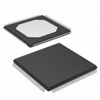
XC3S200-4TQG144I Xilinx Inc, XC3S200-4TQG144I Datasheet - Page 53

XC3S200-4TQG144I
Manufacturer Part Number
XC3S200-4TQG144I
Description
FPGA Spartan®-3 Family 200K Gates 4320 Cells 630MHz 90nm Technology 1.2V 144-Pin TQFP
Manufacturer
Xilinx Inc
Series
Spartan™-3r
Datasheet
1.XC3S50-4VQG100C.pdf
(217 pages)
Specifications of XC3S200-4TQG144I
Package
144TQFP
Family Name
Spartan®-3
Device Logic Units
4320
Device System Gates
200000
Maximum Internal Frequency
630 MHz
Typical Operating Supply Voltage
1.2 V
Maximum Number Of User I/os
97
Ram Bits
221184
Package / Case
144-TQFP, 144-VQFP
Mounting Type
Surface Mount
Voltage - Supply
1.14 V ~ 3.465 V
Operating Temperature
-40°C ~ 100°C
Number Of I /o
97
Number Of Logic Elements/cells
*
Number Of Gates
*
Lead Free Status / RoHS Status
Lead free / RoHS Compliant
Available stocks
Company
Part Number
Manufacturer
Quantity
Price
Company:
Part Number:
XC3S200-4TQG144I
Manufacturer:
XILINX
Quantity:
1 029
threshold levels (see
plies reach their respective threshold, the POR reset is
released and the FPGA begins its configuration process.
Because the three supply inputs must be valid to release
the POR reset and can be supplied in any order, there are
no specific voltage sequencing requirements. However,
applying the FPGA’s V
ply uses the least I
Once all three supplies are valid, the minimum current
required to power-on the FPGA is equal to the worst-case
quiescent current, as specified in
tan-3 FPGAs do not require Power-On Surge (POS) current
to successfully configure.
Surplus I
If the V
the FPGA may draw a surplus I
the I
The momentary additional I
few hundred milliamperes under nominal conditions, signifi-
cantly less than the instantaneous current consumed by the
bypass capacitors at power-on. However, the surplus cur-
rent immediately disappears when the V
applied, and, in response, the FPGA’s I
rent demand drops to the levels specified in
FPGA does not use nor does it require the surplus current
to successfully power-on and configure. If applying V
before V
foldback feature that could inadvertently shut down in the
presence of the surplus current.
Maximum Allowed V
Devices, if V
All devices with a mask revision code ‘E’ or later do not have
a V
sions, page
Early Spartan-3 FPGAs were produced at a 200 mm wafer
production facility and are identified by a fabrication/process
code of "FQ" on the device top marking, as shown in
age Marking, page
mum V
the last supply to ramp, after the V
supplies. This maximum ramp rate appears as T
Table 29, page
Minimum Allowed V
Devices
Devices shipped since 2006 essentially have no V
rate limits, shown in
with a mask revision code ‘E’ or later do not have a V
ramp rate limit. See
DS099-2 (v2.5) December 4, 2009
Product Specification
CCINT
CCINT
CCINT
CCINT
CCAUX
ramp rate requirement. See
CCINT
quiescent current levels specified in
R
55.
ramp rate requirement if and only if V
supply is applied before the V
VCCINT
, ensure that the regulator does not have a
57.
if V
CCINT
Table 29, page
Mask and Fab Revisions, page
7. These "FQ" devices have a maxi-
Table 28, page
CCINT
Supply is Last in Sequence
CCAUX
CCINT
current.
CCO
CCINT
Applied before V
supply before the V
Ramp Rate on Early
CCINT
Ramp Rate on Early
surplus current might be a
Table 33, page
CCAUX
57. Similarly, all devices
56). After all three sup-
Mask and Fab Revi-
current in addition to
CCINT
and V
CCAUX
CCAUX
quiescent cur-
Table
CCO
CCAUX
CCINT
CCO
60. Spar-
supply is
Table
CCINT
CCINT
33. The
Bank 4
supply,
CCINT
Pack-
55.
www.xilinx.com
ramp
sup-
CCO
33.
in
is
-
Initial Spartan-3 FPGA mask revisions have a limit on how
fast the V
ramp rate appears as T
mum rate is affected by the package inductance. Conse-
quently, the ball grid array and chip-scale packages
(CP132, FT256, FG456, FG676, and FG900) allow a faster
ramp rate than the quad-flat packages (VQ100, TQ144, and
PQ208).
Configuration Data Retention, Brown-Out
The FPGA’s configuration data is stored in robust CMOS
configuration latches. The data in these latches is retained
even when the voltages drop to the minimum levels neces-
sary to preserve RAM contents. This is specified in
Table 30, page
If, after configuration, the V
below its data retention voltage, clear the current device
configuration using one of the following methods:
•
•
The POR circuit does not monitor the VCCO_4 supply after
configuration. Consequently, dropping the VCCO_4 voltage
does not reset the device by triggering a Power-On Reset
(POR) event.
No Internal Charge Pumps or Free-Running
Oscillators
Some system applications are sensitive to sources of ana-
log noise. Spartan-3 FPGA circuitry is fully static and does
not employ internal charge pumps.
The CCLK configuration clock is active during the FPGA
configuration process. After configuration completes, the
CCLK oscillator is automatically disabled unless the Bit-
stream Generator (BitGen) option Persist=Yes. See Mod-
ule 4:
Spartan-3 FPGAs optionally support a featured called
tally Controlled Impedance
cation, the DCI logic uses an internal oscillator. The DCI
logic is only enabled if the FPGA application specifies an I/O
standard that requires DCI (LVDCI_33, LVDCI_25, etc.). If
DCI is not used, the associated internal oscillator is also dis-
abled.
In summary, unless an application uses the Persist=Yes
option or specifies a DCI I/O standard, an FPGA with no
external switching remains fully static.
Force the V
minimum Power On Reset (POR) voltage threshold
Table 28, page
Assert PROG_B Low.
Table 79, page
Spartan-3 FPGA Family: Functional Description
CCO
supply can ramp. The minimum allowed V
57.
CCAUX
56).
117.
or V
CCO
CCINT
CCAUX
in
(DCI). When used in an appli-
Table 29, page
supply voltage below the
or V
CCINT
57. The mini-
supply drops
Digi-
CCO
53


