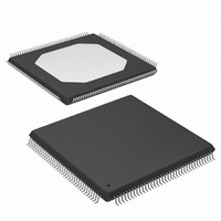
XC3S200-4TQG144I Xilinx Inc, XC3S200-4TQG144I Datasheet - Page 35

XC3S200-4TQG144I
Manufacturer Part Number
XC3S200-4TQG144I
Description
FPGA Spartan®-3 Family 200K Gates 4320 Cells 630MHz 90nm Technology 1.2V 144-Pin TQFP
Manufacturer
Xilinx Inc
Series
Spartan™-3r
Datasheet
1.XC3S50-4VQG100C.pdf
(217 pages)
Specifications of XC3S200-4TQG144I
Package
144TQFP
Family Name
Spartan®-3
Device Logic Units
4320
Device System Gates
200000
Maximum Internal Frequency
630 MHz
Typical Operating Supply Voltage
1.2 V
Maximum Number Of User I/os
97
Ram Bits
221184
Package / Case
144-TQFP, 144-VQFP
Mounting Type
Surface Mount
Voltage - Supply
1.14 V ~ 3.465 V
Operating Temperature
-40°C ~ 100°C
Number Of I /o
97
Number Of Logic Elements/cells
*
Number Of Gates
*
Lead Free Status / RoHS Status
Lead free / RoHS Compliant
Available stocks
Company
Part Number
Manufacturer
Quantity
Price
Company:
Part Number:
XC3S200-4TQG144I
Manufacturer:
XILINX
Quantity:
1 029
In the on-chip synchronization case
Figure
output clock signals through general routing resources to
the FPGA’s internal registers. Either a Global Clock Buffer
(BUFG) or a BUFGMUX affords access to the global clock
network. As shown in
ated by routing CLK0 (or CLK2X, in
clock net, which in turn drives the CLKFB input.
In the off-chip synchronization case
Figure
output clock signals exit the FPGA using output buffers
(OBUF) to drive an external clock network plus registers on
the board. As shown in
formed by feeding CLK0 (or CLK2X, in
into the FPGA using an IBUFG, which directly accesses the
global clock network, or an IBUF. Then, the global clock net
is connected directly to the CLKFB input.
DLL Frequency Modes
The DLL supports two distinct operating modes, High Fre-
quency and Low Frequency, with each specified over a differ-
ent clock frequency range. The DLL_FREQUENCY_MODE
DS099-2 (v2.5) December 4, 2009
Product Specification
Notes:
1.
19b), it is possible to connect any of the DLL’s seven
19d), CLK0 (or CLK2X) plus any of the DLL’s other
BUFG
In the Low Frequency mode, all seven DLL outputs are available. In the High Frequency mode, only the CLK0, CLK180,
and CLKDV outputs are available.
R
IBUFG
IBUFG
(c) Off-Chip with CLK0 Feedback
(a) On-Chip with CLK0 Feedback
Figure 19: Input Clock, Output Clock, and Feedback Connections for the DLL
CLKIN
CLKFB
CLKIN
CLKFB
DCM
DCM
Figure
FPGA
Figure
CLK2X180
CLK2X180
FPGA
CLK0
CLK0
CLK180
CLK270
CLK180
CLK270
CLKDV
CLKDV
CLK2X
CLK2X
19a, the feedback loop is cre-
CLK90
CLK90
CLK0
CLK0
19c, the feedback loop is
Figure
BUFGMUX
BUFGMUX
OBUF
OBUF
Figure
(Figure 19a
(Figure 19c
19b) to a global
Net Delay
Clock
Net Delay
Clock
19d) back
www.xilinx.com
and
and
attribute chooses between the two modes. When the
attribute is set to LOW, the Low Frequency mode permits all
seven DLL clock outputs to operate over a low-to-moderate
frequency range. When the attribute is set to HIGH, the High
Frequency mode allows the CLK0, CLK180 and CLKDV out-
puts to operate at the highest possible frequencies. The
remaining DLL clock outputs are not available for use in High
Frequency mode.
Accommodating High Input Frequencies
If the frequency of the CLKIN signal is high such that it
exceeds the maximum permitted, divide it down to an
acceptable value using the CLKIN_DIVIDE_BY_2 attribute.
When this attribute is set to TRUE, the CLKIN frequency is
divided by a factor of two just as it enters the DCM.
Coarse Phase Shift Outputs of the DLL Compo-
nent
In addition to CLK0 for zero-phase alignment to the CLKIN
signal, the DLL also provides the CLK90, CLK180 and
CLK270 outputs for 90°, 180° and 270° phase-shifted sig-
nals, respectively. These signals are described in
BUFG
IBUFG
IBUFG
Spartan-3 FPGA Family: Functional Description
(d) Off-Chip with CLK2X Feedback
(b) On-Chip with CLK2X Feedback
CLKIN
CLKFB
CLKIN
CLKFB
DCM
DCM
FPGA
CLK2X180
CLK2X180
CLK2X
CLK2X
FPGA
CLK180
CLK270
CLK180
CLK270
CLKDV
CLKDV
CLK90
CLK90
CLK2X
CLK0
CLK2X
CLK0
BUFGMUX
BUFGMUX
OBUF
OBUF
Net Delay
Clock
Net Delay
DS099-2_09_082104
Clock
Table
15.
35


