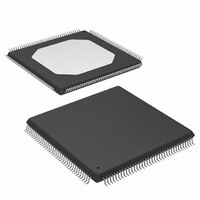
XC3S200-4TQG144I Xilinx Inc, XC3S200-4TQG144I Datasheet - Page 34

XC3S200-4TQG144I
Manufacturer Part Number
XC3S200-4TQG144I
Description
FPGA Spartan®-3 Family 200K Gates 4320 Cells 630MHz 90nm Technology 1.2V 144-Pin TQFP
Manufacturer
Xilinx Inc
Series
Spartan™-3r
Datasheet
1.XC3S50-4VQG100C.pdf
(217 pages)
Specifications of XC3S200-4TQG144I
Package
144TQFP
Family Name
Spartan®-3
Device Logic Units
4320
Device System Gates
200000
Maximum Internal Frequency
630 MHz
Typical Operating Supply Voltage
1.2 V
Maximum Number Of User I/os
97
Ram Bits
221184
Package / Case
144-TQFP, 144-VQFP
Mounting Type
Surface Mount
Voltage - Supply
1.14 V ~ 3.465 V
Operating Temperature
-40°C ~ 100°C
Number Of I /o
97
Number Of Logic Elements/cells
*
Number Of Gates
*
Lead Free Status / RoHS Status
Lead free / RoHS Compliant
Available stocks
Company
Part Number
Manufacturer
Quantity
Price
Company:
Part Number:
XC3S200-4TQG144I
Manufacturer:
XILINX
Quantity:
1 029
Spartan-3 FPGA Family: Functional Description
Table 16: DLL Attributes
DLL Clock Input Connections
An external clock source enters the FPGA using a Global
Clock Input Buffer (IBUFG), which directly accesses the glo-
bal clock network or an Input Buffer (IBUF). Clock signals
within the FPGA drive a global clock net using a Global
Clock Multiplexer Buffer (BUFGMUX). The global clock net
connects directly to the CLKIN input. The internal and exter-
nal connections are shown in
respectively. A differential clock (e.g., LVDS) can serve as
an input to CLKIN.
DLL Clock Output and Feedback Connections
As many as four of the nine DCM clock outputs can simulta-
neously drive the four BUFGMUX buffers on the same die
edge (top or bottom). All DCM clock outputs can simulta-
neously drive general routing resources, including intercon-
nect leading to OBUF buffers.
The feedback loop is essential for DLL operation and is
established by driving the CLKFB input with either the CLK0
34
54
CLK_FEEDBACK
DLL_FREQUENCY_MODE
CLKIN_DIVIDE_BY_2
CLKDV_DIVIDE
DUTY_CYCLE_CORRECTION
Attribute
Figure 19a
Chooses either the CLK0 or CLK2X output to drive the
CLKFB input
Chooses between High Frequency and Low
Frequency modes
Halves the frequency of the CLKIN signal just as it
enters the DCM
Selects constant used to divide the CLKIN input
frequency to generate the CLKDV output frequency
Enables 50% duty cycle correction for the CLK0,
CLK90, CLK180, and CLK270 outputs
and
Figure
www.xilinx.com
19c,
Description
or the CLK2X signal so that any undesirable clock distribu-
tion delay is included in the loop. It is possible to use either
of these two signals for synchronizing any of the seven DLL
outputs: CLK0, CLK90, CLK180, CLK270, CLKDV, CLK2X,
or CLK2X180. The value assigned to the CLK_FEEDBACK
attribute must agree with the physical feedback connection:
a value of 1X for the CLK0 case, 2X for the CLK2X case. If
the DCM is used in an application that does not require the
DLL — i.e., only the DFS is used — then there is no feed-
back loop so CLK_FEEDBACK is set to NONE.
CLK2X feedback is only supported on all mask revision ‘E’
and later devices (see
on devices with the "GQ" fabrication code, and on all ver-
sions of the XC3S50 and XC3S1000.
There are two basic cases that determine how to connect
the DLL clock outputs and feedback connections: on-chip
synchronization and off-chip synchronization, which are
illustrated in
Figure 19a
Mask and Fab Revisions, page
through
DS099-2 (v2.5) December 4, 2009
NONE, 1X, 2X
LOW, HIGH
TRUE, FALSE
1.5, 2, 2.5, 3, 3.5, 4, 4.5, 5, 5.5,
6.0, 6.5, 7.0, 7.5, 8, 9, 10, 11,
12, 13, 14, 15, and 16.
TRUE, FALSE
Figure
Product Specification
19d.
Values
55),
R


