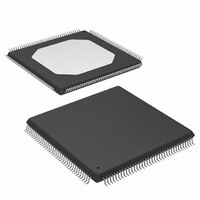
XC3S200-4TQG144I Xilinx Inc, XC3S200-4TQG144I Datasheet - Page 56

XC3S200-4TQG144I
Manufacturer Part Number
XC3S200-4TQG144I
Description
FPGA Spartan®-3 Family 200K Gates 4320 Cells 630MHz 90nm Technology 1.2V 144-Pin TQFP
Manufacturer
Xilinx Inc
Series
Spartan™-3r
Datasheet
1.XC3S50-4VQG100C.pdf
(217 pages)
Specifications of XC3S200-4TQG144I
Package
144TQFP
Family Name
Spartan®-3
Device Logic Units
4320
Device System Gates
200000
Maximum Internal Frequency
630 MHz
Typical Operating Supply Voltage
1.2 V
Maximum Number Of User I/os
97
Ram Bits
221184
Package / Case
144-TQFP, 144-VQFP
Mounting Type
Surface Mount
Voltage - Supply
1.14 V ~ 3.465 V
Operating Temperature
-40°C ~ 100°C
Number Of I /o
97
Number Of Logic Elements/cells
*
Number Of Gates
*
Lead Free Status / RoHS Status
Lead free / RoHS Compliant
Available stocks
Company
Part Number
Manufacturer
Quantity
Price
Company:
Part Number:
XC3S200-4TQG144I
Manufacturer:
XILINX
Quantity:
1 029
Spartan-3 FPGA Family: DC and Switching Characteristics
Table 27: Absolute Maximum Ratings (Continued)
Table 28: Supply Voltage Thresholds for Power-On Reset
56
Notes:
1.
2.
3.
4.
Notes:
1.
2.
3.
Symbol
V
T
T
T
STG
I
ESD
SOL
Stresses beyond those listed under Absolute Maximum Ratings may cause permanent damage to the device. These are stress
ratings only; functional operation of the device at these or any other conditions beyond those listed under the Recommended
Operating Conditions is not implied. Exposure to Absolute Maximum Ratings conditions for extended periods of time adversely
affects device reliability.
All User I/O and Dual-Purpose pins (DIN/D0, D1–D7, CS_B, RDWR_B, BUSY/DOUT, and INIT_B) draw power from the V
rail of the associated bank. Keeping V
junctions that exist between each of these pins and the V
to determine the max limit. Input voltages outside the -0.5V to V
clamp diode rating is met and no more than 100 pins exceed the range simultaneously. Prolonged exposure to such current may
compromise device reliability. A sustained current of 10 mA will not compromise device reliability. See XAPP459, Eliminating I/O
Coupling Effects when Interfacing Large-Swing Single-Ended Signals to User I/O Pins on Spartan-3 Generation FPGAs for more
details. The V
to handle overshoot/undershoot as well as achieve PCI compliance. Refer to the following application notes: XAPP457, Powering
and Configuring Spartan-3 Generation FPGAs in Compliant PCI Applications and XAPP659, Virtex
Design Guidelines.
All Dedicated pins (M0–M2, CCLK, PROG_B, DONE, HSWAP_EN, TCK, TDI, TDO, and TMS) draw power from the V
(2.5V). Meeting the V
do not turn on.
operating level (2.625V), V
concerning the use of 3.3V signals, see the
For soldering guidelines, see UG112, Device Packaging and Thermal Characteristics and XAPP427, Implementation and Solder
Reflow Guidelines for Pb-Free Packages.
V
draw a surplus current in addition to the quiescent current levels specified in
current. The FPGA does not use any of the surplus current for the power-on process. For this power sequence, make sure that
regulators with foldback features will not shut down inadvertently.
To ensure successful power-on, V
ranges with no dips at any point.
If a brown-out condition occurs where V
V
IK
J
CCINT
CCINT
V
Symbol
V
V
CCAUXT
CCINTT
CCO4T
, V
must drop below the minimum power-on reset voltage in order to clear out the device configuration content.
Input clamp current per I/O pin
Electrostatic Discharge Voltage pins relative
to GND
Junction temperature
Soldering temperature
Storage temperature
CCAUX
IN
Table 31
, and V
limits apply to both the DC and AC components of signals. Simple application solutions are available that show how
Threshold for the V
Threshold for the V
Threshold for the V
IN
CCO
max limit ensures that the internal diode junctions that exist between each of these pins and the V
specifies the V
Description
IN
supplies may be applied in any order. When applying V
max < 3.125V. As long as the V
CCINT
IN
CCAUX
, V
CCAUX
within 500 mV of the associated V
CCINT
CCAUX
CCO
CCO
3.3V-Tolerant Configuration Interface, page
Description
range used to determine the max limit. When V
Bank 4, and V
or V
Bank 4 supply
supply
supply
CCINT
–0.5 V
Human body model
Charged device model
Machine model
www.xilinx.com
CCO
drops below the retention voltage indicated in
IN
and GND rails do not turn on.
CCAUX
< V
max specification is met, oxide stress is not possible. For information
CCO
IN
Conditions
+0.5V voltage range are permissible provided that the I
supplies must rise through their respective threshold-voltage
< (V
CCO
CCO
Table
+ 0.5 V)
rails or ground rail ensures that the internal diode
CCINT
33. Applying V
power before V
Min
0.4
0.8
0.4
Table 31
46. See XAPP459.
CCAUX
Min
DS099-3 (v2.5) December 4, 2009
–65
CCAUX
is at its maximum recommended
®
-
-
-
-
-
specifies the V
-II Pro / Virtex-II Pro X 3.3V I/O
CCAUX
Table
eliminates the surplus
Max
1.0
2.0
1.0
Product Specification
power, the FPGA may
30, then V
±2000
±100
±500
±200
Max
125
220
150
CCO
CCAUX
range used
CCO
CCAUX
CCAUX
Units
IK
V
V
V
Units
power
mA
input
rail
°C
°C
°C
V
V
V
or
rail
R


