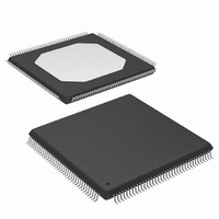
XC3S200-4TQG144I Xilinx Inc, XC3S200-4TQG144I Datasheet - Page 135

XC3S200-4TQG144I
Manufacturer Part Number
XC3S200-4TQG144I
Description
FPGA Spartan®-3 Family 200K Gates 4320 Cells 630MHz 90nm Technology 1.2V 144-Pin TQFP
Manufacturer
Xilinx Inc
Series
Spartan™-3r
Datasheet
1.XC3S50-4VQG100C.pdf
(217 pages)
Specifications of XC3S200-4TQG144I
Package
144TQFP
Family Name
Spartan®-3
Device Logic Units
4320
Device System Gates
200000
Maximum Internal Frequency
630 MHz
Typical Operating Supply Voltage
1.2 V
Maximum Number Of User I/os
97
Ram Bits
221184
Package / Case
144-TQFP, 144-VQFP
Mounting Type
Surface Mount
Voltage - Supply
1.14 V ~ 3.465 V
Operating Temperature
-40°C ~ 100°C
Number Of I /o
97
Number Of Logic Elements/cells
*
Number Of Gates
*
Lead Free Status / RoHS Status
Lead free / RoHS Compliant
Available stocks
Company
Part Number
Manufacturer
Quantity
Price
Company:
Part Number:
XC3S200-4TQG144I
Manufacturer:
XILINX
Quantity:
1 029
PQ208: 208-lead Plastic Quad Flat Pack
The 208-lead plastic quad flat package, PQ208, supports
three different Spartan-3 devices, including the XC3S50,
the XC3S200, and the XC3S400. The footprints for the
XC3S200 and XC3S400 are identical, as shown in
and
resulting in 17 unconnected pins on the PQ208 package,
labeled as “N.C.” In
nected pins are indicated with a black diamond symbol ( ).
All the package pins appear in
bank number, then by pin name. Pairs of pins that form a dif-
ferential I/O pair appear together in the table. The table also
shows the pin number for each pin and the pin type, as
defined earlier.
If there is a difference between the XC3S50 pinout and the
pinout for the XC3S200 and XC3S400, then that difference
is highlighted in
then there is an unconnected pin on the XC3S50 that maps
to a user-I/O pin on the XC3S200 and XC3S400. If the table
entry is shaded tan, then the unconnected pin on the
XC3S50 maps to a VREF-type pin on the XC3S200 and
XC3S400. If the other VREF pins in the bank all connect to
a voltage reference to support a special I/O standard, then
also connect the N.C. pin on the XC3S50 to the same VREF
voltage. This provides maximum flexibility as you could
potentially migrate a design from the XC3S50 device to an
XC3S200 or XC3S400 FPGA without changing the printed
circuit board.
An electronic version of this package pinout table and foot-
print diagram is available for download from the Xilinx web-
site at
sheets/s3_pin.zip
Pinout Table
Table 92: PQ208 Package Pinout
DS099-4 (v2.5) December 4, 2009
Product Specification
Bank
Figure
0
0
0
0
0
0
0
0
0
0
0
http://www.xilinx.com/support/documentation/data_
IO
IO
N.C. ( )
IO/VREF_0
IO_L01N_0/
VRP_0
IO_L01P_0/
VRN_0
IO_L25N_0
IO_L25P_0
IO_L27N_0
IO_L27P_0
IO_L30N_0
45. The XC3S50, however, has fewer I/O pins
R
Pin Name
XC3S50
Table
.
Table 92
92. If the table entry is shaded grey,
IO
IO
IO/VREF_0
IO/VREF_0
IO_L01N_0/
VRP_0
IO_L01P_0/
VRN_0
IO_L25N_0
IO_L25P_0
IO_L27N_0
IO_L27P_0
IO_L30N_0
Pin Name
XC3S200
XC3S400
and
Table 92
Figure
Number
PQ208
and are sorted by
P189
P197
P200
P205
P204
P203
P199
P198
P196
P194
P191
45, these uncon-
Pin
Table 92
VREF
VREF
Type
DCI
DCI
I/O
I/O
I/O
I/O
I/O
I/O
I/O
www.xilinx.com
Table 92: PQ208 Package Pinout (Continued)
Bank
0
0
0
0
0
0
0
1
1
1
1
1
1
1
1
1
1
1
1
1
1
1
1
1
2
2
2
2
2
2
2
2
2
2
Spartan-3 FPGA Family: Pinout Descriptions
IO_L30P_0
IO_L31N_0
IO_L31P_0/
VREF_0
IO_L32N_0/
GCLK7
IO_L32P_0/
GCLK6
VCCO_0
VCCO_0
IO
IO
IO
IO_L01N_1/
VRP_1
IO_L01P_1/
VRN_1
IO_L10N_1/
VREF_1
IO_L10P_1
IO_L27N_1
IO_L27P_1
IO_L28N_1
IO_L28P_1
IO_L31N_1/
VREF_1
IO_L31P_1
IO_L32N_1/
GCLK5
IO_L32P_1/
GCLK4
VCCO_1
VCCO_1
N.C. ( )
IO_L01N_2/
VRP_2
IO_L01P_2/
VRN_2
IO_L19N_2
IO_L19P_2
IO_L20N_2
IO_L20P_2
IO_L21N_2
IO_L21P_2
IO_L22N_2
Pin Name
XC3S50
IO_L30P_0
IO_L31N_0
IO_L31P_0/
VREF_0
IO_L32N_0/
GCLK7
IO_L32P_0/
GCLK6
VCCO_0
VCCO_0
IO
IO
IO
IO_L01N_1/
VRP_1
IO_L01P_1/
VRN_1
IO_L10N_1/
VREF_1
IO_L10P_1
IO_L27N_1
IO_L27P_1
IO_L28N_1
IO_L28P_1
IO_L31N_1/
VREF_1
IO_L31P_1
IO_L32N_1/
GCLK5
IO_L32P_1/
GCLK4
VCCO_1
VCCO_1
IO/VREF_2
IO_L01N_2/
VRP_2
IO_L01P_2/
VRN_2
IO_L19N_2
IO_L19P_2
IO_L20N_2
IO_L20P_2
IO_L21N_2
IO_L21P_2
IO_L22N_2
Pin Name
XC3S200
XC3S400
Number
PQ208
P190
P187
P185
P184
P183
P188
P201
P167
P175
P182
P162
P161
P166
P165
P169
P168
P172
P171
P178
P176
P181
P180
P164
P177
P154
P156
P155
P152
P150
P149
P148
P147
P146
P144
Pin
VCCO
VCCO
VCCO
VCCO
VREF
GCLK
GCLK
VREF
VREF
GCLK
GCLK
VREF
Type
DCI
DCI
DCI
DCI
I/O
I/O
I/O
I/O
I/O
I/O
I/O
I/O
I/O
I/O
I/O
I/O
I/O
I/O
I/O
I/O
I/O
I/O
135


