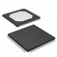
XC3S200-4TQG144I Xilinx Inc, XC3S200-4TQG144I Datasheet - Page 28

XC3S200-4TQG144I
Manufacturer Part Number
XC3S200-4TQG144I
Description
FPGA Spartan®-3 Family 200K Gates 4320 Cells 630MHz 90nm Technology 1.2V 144-Pin TQFP
Manufacturer
Xilinx Inc
Series
Spartan™-3r
Datasheet
1.XC3S50-4VQG100C.pdf
(217 pages)
Specifications of XC3S200-4TQG144I
Package
144TQFP
Family Name
Spartan®-3
Device Logic Units
4320
Device System Gates
200000
Maximum Internal Frequency
630 MHz
Typical Operating Supply Voltage
1.2 V
Maximum Number Of User I/os
97
Ram Bits
221184
Package / Case
144-TQFP, 144-VQFP
Mounting Type
Surface Mount
Voltage - Supply
1.14 V ~ 3.465 V
Operating Temperature
-40°C ~ 100°C
Number Of I /o
97
Number Of Logic Elements/cells
*
Number Of Gates
*
Lead Free Status / RoHS Status
Lead free / RoHS Compliant
Available stocks
Company
Part Number
Manufacturer
Quantity
Price
Company:
Part Number:
XC3S200-4TQG144I
Manufacturer:
XILINX
Quantity:
1 029
Spartan-3 FPGA Family: Functional Description
Port Aspect Ratios
On a given port, it is possible to select a number of different
possible widths (w – p) for the DI/DO buses as shown in
Table
This data bus width selection is independent for each port. If
the data bus width of Port A differs from that of Port B, the
Block RAM automatically performs a bus-matching function.
When data are written to a port with a narrow bus, then read
from a port with a wide bus, the latter port will effectively
combine “narrow” words to form “wide” words. Similarly,
when data are written into a port with a wide bus, then read
from a port with a narrow bus, the latter port will divide
“wide” words to form “narrow” words. When the data bus
width is eight bits or greater, extra parity bits become avail-
able. The width of the total data path (w) is the sum of the
DI/DO bus width and any parity bits (p).
Table 13: Port Aspect Ratios for Port A or B
Block RAM Data Operations
Writing data to and accessing data from the block RAM are
synchronous operations that take place independently on
each of the two ports.
The waveforms for the write operation are shown in the top
half of the
WE and EN signals enable the active edge of CLK, data at
the DI input bus is written to the block RAM location
addressed by the ADDR lines.
There are a number of different conditions under which data
can be accessed at the DO outputs. Basic data access
always occurs when the WE input is inactive. Under this
condition, data stored in the memory location addressed by
28
54
DI/DO Bus Width
(w – p bits)
13. These two buses always have the same width.
16
32
1
2
4
8
Figure
13,
Figure
Bus Width (p bits)
DIP/DOP
14, and
0
0
0
1
2
4
Figure
15. When the
Total Data Path
Width (w bits)
18
36
www.xilinx.com
1
2
4
9
The width selection made for the DI/DO bus determines the
number of address lines according to the relationship
expressed below:
In turn, the number of address lines delimits the total num-
ber (n) of addressable locations or depth according to the
following equation:
The product of w and n yields the total block RAM capacity.
Equations (1) and (2) show that as the data bus width
increases, the number of address lines along with the num-
ber of addressable memory locations decreases. Using the
permissible DI/DO bus widths as inputs to these equations
provides the bus width and memory capacity measures
shown in
the ADDR lines passes through a transparent output latch
to the DO outputs. The timing for basic data access is
shown in the portions of
Figure 15
Data can also be accessed on the DO outputs when assert-
ing the WE input. This is accomplished using two different
attributes:
Choosing the WRITE_FIRST attribute, data is written to the
addressed memory location on an enabled active CLK edge
and is also passed to the DO outputs. WRITE_FIRST timing
is shown in the portion of
High.
Width (r bits)
ADDR Bus
Table
during which WE is Low.
14
13
12
11
10
9
r = 14 – [log(w–p)/log(2)]
13.
n = 2
Locations (n)
Addressable
Figure 13
DS099-2 (v2.5) December 4, 2009
r
16,384
No. of
8,192
4,096
2,048
1,024
512
Figure
13,
Product Specification
during which WE is
Figure
Block RAM
Capacity
16,384
16,384
16,384
18,432
18,432
18,432
(bits)
14, and
(1)
(2)
R


