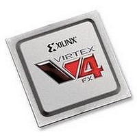
XC4VFX20-10FFG672C Xilinx Inc, XC4VFX20-10FFG672C Datasheet - Page 105

XC4VFX20-10FFG672C
Manufacturer Part Number
XC4VFX20-10FFG672C
Description
IC FPGA VIRTEX-4 FX 20K 672-FBGA
Manufacturer
Xilinx Inc
Series
Virtex™-4r
Datasheets
1.XC4VFX12-10FFG668C.pdf
(58 pages)
2.XC4VFX12-10FFG668C.pdf
(9 pages)
3.XC4VFX12-10FFG668C.pdf
(406 pages)
Specifications of XC4VFX20-10FFG672C
Total Ram Bits
1253376
Number Of Logic Elements/cells
19224
Number Of Labs/clbs
2136
Number Of I /o
320
Voltage - Supply
1.14 V ~ 1.26 V
Mounting Type
Surface Mount
Operating Temperature
0°C ~ 85°C
Package / Case
672-BBGA, FCBGA
No. Of Logic Blocks
19224
No. Of Macrocells
19224
No. Of Speed Grades
10
No. Of I/o's
320
Clock Management
DCM
I/o Supply Voltage
3.45V
Lead Free Status / RoHS Status
Lead free / RoHS Compliant
For Use With
HW-V4-ML405-UNI-G - EVALUATION PLATFORM VIRTEX-4
Number Of Gates
-
Lead Free Status / RoHS Status
Lead free / RoHS Compliant, Lead free / RoHS Compliant
Available stocks
Company
Part Number
Manufacturer
Quantity
Price
Company:
Part Number:
XC4VFX20-10FFG672C
Manufacturer:
ADVANTEK
Quantity:
314
Company:
Part Number:
XC4VFX20-10FFG672C
Manufacturer:
XilinxInc
Quantity:
3 000
Company:
Part Number:
XC4VFX20-10FFG672C
Manufacturer:
Xilinx Inc
Quantity:
10 000
Part Number:
XC4VFX20-10FFG672C
Manufacturer:
XILINX/赛灵思
Quantity:
20 000
- XC4VFX12-10FFG668C PDF datasheet
- XC4VFX12-10FFG668C PDF datasheet #2
- XC4VFX12-10FFG668C PDF datasheet #3
- Current page: 105 of 406
- Download datasheet (6Mb)
Virtex-4 FPGA User Guide
UG070 (v2.6) December 1, 2008
Connecting PMCD to other Clock Resources
R
IBUFG to PMCD
DCM to PMCD
BUFGCTRL to PMCD
Figure 3-6
In most applications, the PMCD is used with other clock resources including dedicated
clock I/O (IBUFG), clock buffers (BUFGCTRLs), DCMs, and an MGT clock. Additionally,
PMCD inputs and outputs can be connected to the general interconnects. This section
provides guidelines on connecting a PMCD to clock resources using dedicated routing.
Virtex-4 devices contain 16 or 32 global clock I/Os. These clock I/Os are accessible by
instantiating the IBUFG component. Each top and bottom half of the center column
contains eight or 16 IBUFGs. Any of the IBUFGs in the top or bottom half can drive the
clock input pins (CLKA, CLKB, CLKC, or CLKD) of a PMCD located in the same
top/bottom half. The routing from multiple IBUFGs to PMCD inputs are not matched.
Any DCM clock output can drive any PMCD input in the same top/bottom half of the
device. A DCM can drive parallel PMCDs in the same group of two. It is not advisable to
drive parallel PMCDs with DCMs in different groups of two (on the same top/bottom
half) because there can be significant skew between PMCD outputs. This skew is caused by
the skew between inputs of PMCDs in different groups.
Any BUFGCTRL can drive any Virtex-4 FPGA PMCD. However, only up to eight
dedicated global clock routing resources exist in a particular clock region. Therefore, access
to PMCD inputs via a BUFGCTRL is limited to eight unique signals. Other resources in the
clock region will compete for the eight global clock tracks.
CLKA1D(2, 4, 8)
CLKA1
CLKA
Deasserted RST
RST
REL
illustrates the interaction between the RST and REL signals.
is registered.
Delayed output clocks start toggling.
Figure 3-6: REL Waveform Example
www.xilinx.com
PMCD Usage and Design Guidelines
Release is synchronized.
Divided output clocks start toggling.
RST_DEASSERT_CLK = CLKA
EN_REL = TRUE
UG070_3_06_071404
105
Related parts for XC4VFX20-10FFG672C
Image
Part Number
Description
Manufacturer
Datasheet
Request
R

Part Number:
Description:
IC FPGA VIRTEX-4 FX 20K 672-FBGA
Manufacturer:
Xilinx Inc
Datasheet:

Part Number:
Description:
IC FPGA VIRTEX-4 FX 20K 672-FBGA
Manufacturer:
Xilinx Inc
Datasheet:

Part Number:
Description:
IC FPGA VIRTEX-4FX 672FFBGA
Manufacturer:
Xilinx Inc
Datasheet:

Part Number:
Description:
IC FPGA VIRTEX-4 FX 20K 672-FBGA
Manufacturer:
Xilinx Inc
Datasheet:

Part Number:
Description:
IC FPGA VIRTEX-4FX 672FFBGA
Manufacturer:
Xilinx Inc
Datasheet:

Part Number:
Description:
DC and Switching Characteristics
Manufacturer:
XILINX [Xilinx, Inc]
Datasheet:

Part Number:
Description:
IC CPLD .8K 36MCELL 44-VQFP
Manufacturer:
Xilinx Inc
Datasheet:

Part Number:
Description:
IC CPLD 72MCRCELL 10NS 44VQFP
Manufacturer:
Xilinx Inc
Datasheet:

Part Number:
Description:
IC CPLD 1.6K 72MCELL 64-VQFP
Manufacturer:
Xilinx Inc
Datasheet:

Part Number:
Description:
IC CR-II CPLD 64MCELL 44-VQFP
Manufacturer:
Xilinx Inc
Datasheet:

Part Number:
Description:
IC CPLD 1.6K 72MCELL 100-TQFP
Manufacturer:
Xilinx Inc
Datasheet:

Part Number:
Description:
IC CR-II CPLD 64MCELL 56-BGA
Manufacturer:
Xilinx Inc
Datasheet:

Part Number:
Description:
IC CPLD 72MCRCELL 7.5NS 44VQFP
Manufacturer:
Xilinx Inc
Datasheet:

Part Number:
Description:
IC CR-II CPLD 64MCELL 100-VQFP
Manufacturer:
Xilinx Inc
Datasheet:

Part Number:
Description:
IC CPLD 1.6K 72MCELL 100-TQFP
Manufacturer:
Xilinx Inc
Datasheet:


