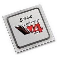
XC4VFX20-10FFG672C Xilinx Inc, XC4VFX20-10FFG672C Datasheet - Page 174

XC4VFX20-10FFG672C
Manufacturer Part Number
XC4VFX20-10FFG672C
Description
IC FPGA VIRTEX-4 FX 20K 672-FBGA
Manufacturer
Xilinx Inc
Series
Virtex™-4r
Datasheets
1.XC4VFX12-10FFG668C.pdf
(58 pages)
2.XC4VFX12-10FFG668C.pdf
(9 pages)
3.XC4VFX12-10FFG668C.pdf
(406 pages)
Specifications of XC4VFX20-10FFG672C
Total Ram Bits
1253376
Number Of Logic Elements/cells
19224
Number Of Labs/clbs
2136
Number Of I /o
320
Voltage - Supply
1.14 V ~ 1.26 V
Mounting Type
Surface Mount
Operating Temperature
0°C ~ 85°C
Package / Case
672-BBGA, FCBGA
No. Of Logic Blocks
19224
No. Of Macrocells
19224
No. Of Speed Grades
10
No. Of I/o's
320
Clock Management
DCM
I/o Supply Voltage
3.45V
Lead Free Status / RoHS Status
Lead free / RoHS Compliant
For Use With
HW-V4-ML405-UNI-G - EVALUATION PLATFORM VIRTEX-4
Number Of Gates
-
Lead Free Status / RoHS Status
Lead free / RoHS Compliant, Lead free / RoHS Compliant
Available stocks
Company
Part Number
Manufacturer
Quantity
Price
Company:
Part Number:
XC4VFX20-10FFG672C
Manufacturer:
ADVANTEK
Quantity:
314
Company:
Part Number:
XC4VFX20-10FFG672C
Manufacturer:
XilinxInc
Quantity:
3 000
Company:
Part Number:
XC4VFX20-10FFG672C
Manufacturer:
Xilinx Inc
Quantity:
10 000
Part Number:
XC4VFX20-10FFG672C
Manufacturer:
XILINX/赛灵思
Quantity:
20 000
- XC4VFX12-10FFG668C PDF datasheet
- XC4VFX12-10FFG668C PDF datasheet #2
- XC4VFX12-10FFG668C PDF datasheet #3
- Current page: 174 of 406
- Download datasheet (6Mb)
Chapter 4: Block RAM
174
[msb:msb-3]
[msb:msb-3]
[msb:msb-3]
WRCOUNT
WRCOUNT
WRCOUNT
Solution 3: FIFO Flag Generator Using Gray Code
Binary → Gray + 1
IN[3:0]
Binary → Gray + 2
IN[3:0]
Binary → Gray + 3
IN[3:0]
Design Description
0000
0001
0010
0011
0100
0101
0110
0111
1000
1001
1010
1011
1100
1101
1110
1111
0000
0001
0010
0011
0100
0101
0110
0111
1000
1001
1010
1011
1100
1101
1110
1111
0000
0001
0010
0011
0100
0101
0110
0111
1000
1001
1010
1011
1100
1101
1110
1111
Figure 4-31: Intermediate Signal Generation for ALMOSTFULL Flag
IN
IN
IN
The incorrect operation of the FIFO16 after a specific sequence of events occurs only on the
flag signals. Once the flag signals are incorrect, the FIFO operation itself can be affected.
In Solution 3, the FIFO flags are generated outside the FIFO16. The externally generated
flags are used in conjunction with the FIFO16 to give the complete FIFO solution. This
solution can also be used if the customer design has the read or write clock stopped in
between during the FIFO operation.
In the solution described here, the FIFO memory address space is divided into 16 sectors.
The number of word in each sector depends on the FIFO depth and is given by FIFO
Depth/ 16. The granularity of this solution is equal to the number of words in each sector.
Four bits are used to identify the 16 sectors within the memory. The four bits are the four
MSB bits of the WRCOUNT signal from the FIFO16.The ALMOSTFULL flag goes true if
the current read sector is equal to the current write sector + 1, 2, or 3. Three binary to gray
code converters uses the four WRCOUNT MSB bits to convert from binary to gray +1, gray
+2, and gray +3 values as shown in
OUT
OUT
OUT
0001
0011
0010
0110
0111
0101
0100
1100
1101
1111
1110
1010
1011
1001
1000
0000
0011
0010
0110
0111
0101
0100
1100
1101
1111
1110
1010
1011
1001
1000
0000
0001
0010
0110
0111
0101
0100
1100
1101
1111
1110
1010
1011
1001
1000
0000
0001
0011
OUT[3:0]
OUT[3:0]
OUT[3:0]
4 LUTs
4 LUTs
4 LUTs
WRCLK
RST
[3:0]
[3:0]
[3:0]
D[3:0] Q[3:0]
D[3:0] Q[3:0]
D[3:0] Q[3:0]
www.xilinx.com
PRE
PRE
PRE
RAgray[3:0]
[3:0]
[3:0]
[3:0]
Figure
4-31.
[1:0]
[1:0]
[3:2]
[3:2]
[1:0]
[1:0]
[3:2]
[3:2]
[1:0]
[1:0]
[3:2]
[3:2]
LUT
LUT
LUT
LUT
LUT
LUT
= =
= =
= =
= =
= =
= =
6 Synchronizers
D
D
D
D
D
D
RST
RST
RST
RST
RST
RST
UG070 (v2.6) December 1, 2008
Q
Q
Q
Q
Q
Q
Virtex-4 FPGA User Guide
LUT
LUT
LUT
UG070_c4_32_020607
D
D
D
RST
RST
RST
Q
Q
Q
AF1
AF2
AF3
R
Related parts for XC4VFX20-10FFG672C
Image
Part Number
Description
Manufacturer
Datasheet
Request
R

Part Number:
Description:
IC FPGA VIRTEX-4 FX 20K 672-FBGA
Manufacturer:
Xilinx Inc
Datasheet:

Part Number:
Description:
IC FPGA VIRTEX-4 FX 20K 672-FBGA
Manufacturer:
Xilinx Inc
Datasheet:

Part Number:
Description:
IC FPGA VIRTEX-4FX 672FFBGA
Manufacturer:
Xilinx Inc
Datasheet:

Part Number:
Description:
IC FPGA VIRTEX-4 FX 20K 672-FBGA
Manufacturer:
Xilinx Inc
Datasheet:

Part Number:
Description:
IC FPGA VIRTEX-4FX 672FFBGA
Manufacturer:
Xilinx Inc
Datasheet:

Part Number:
Description:
DC and Switching Characteristics
Manufacturer:
XILINX [Xilinx, Inc]
Datasheet:

Part Number:
Description:
IC CPLD .8K 36MCELL 44-VQFP
Manufacturer:
Xilinx Inc
Datasheet:

Part Number:
Description:
IC CPLD 72MCRCELL 10NS 44VQFP
Manufacturer:
Xilinx Inc
Datasheet:

Part Number:
Description:
IC CPLD 1.6K 72MCELL 64-VQFP
Manufacturer:
Xilinx Inc
Datasheet:

Part Number:
Description:
IC CR-II CPLD 64MCELL 44-VQFP
Manufacturer:
Xilinx Inc
Datasheet:

Part Number:
Description:
IC CPLD 1.6K 72MCELL 100-TQFP
Manufacturer:
Xilinx Inc
Datasheet:

Part Number:
Description:
IC CR-II CPLD 64MCELL 56-BGA
Manufacturer:
Xilinx Inc
Datasheet:

Part Number:
Description:
IC CPLD 72MCRCELL 7.5NS 44VQFP
Manufacturer:
Xilinx Inc
Datasheet:

Part Number:
Description:
IC CR-II CPLD 64MCELL 100-VQFP
Manufacturer:
Xilinx Inc
Datasheet:

Part Number:
Description:
IC CPLD 1.6K 72MCELL 100-TQFP
Manufacturer:
Xilinx Inc
Datasheet:


