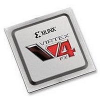
XC4VFX20-10FFG672C Xilinx Inc, XC4VFX20-10FFG672C Datasheet - Page 383

XC4VFX20-10FFG672C
Manufacturer Part Number
XC4VFX20-10FFG672C
Description
IC FPGA VIRTEX-4 FX 20K 672-FBGA
Manufacturer
Xilinx Inc
Series
Virtex™-4r
Datasheets
1.XC4VFX12-10FFG668C.pdf
(58 pages)
2.XC4VFX12-10FFG668C.pdf
(9 pages)
3.XC4VFX12-10FFG668C.pdf
(406 pages)
Specifications of XC4VFX20-10FFG672C
Total Ram Bits
1253376
Number Of Logic Elements/cells
19224
Number Of Labs/clbs
2136
Number Of I /o
320
Voltage - Supply
1.14 V ~ 1.26 V
Mounting Type
Surface Mount
Operating Temperature
0°C ~ 85°C
Package / Case
672-BBGA, FCBGA
No. Of Logic Blocks
19224
No. Of Macrocells
19224
No. Of Speed Grades
10
No. Of I/o's
320
Clock Management
DCM
I/o Supply Voltage
3.45V
Lead Free Status / RoHS Status
Lead free / RoHS Compliant
For Use With
HW-V4-ML405-UNI-G - EVALUATION PLATFORM VIRTEX-4
Number Of Gates
-
Lead Free Status / RoHS Status
Lead free / RoHS Compliant, Lead free / RoHS Compliant
Available stocks
Company
Part Number
Manufacturer
Quantity
Price
Company:
Part Number:
XC4VFX20-10FFG672C
Manufacturer:
ADVANTEK
Quantity:
314
Company:
Part Number:
XC4VFX20-10FFG672C
Manufacturer:
XilinxInc
Quantity:
3 000
Company:
Part Number:
XC4VFX20-10FFG672C
Manufacturer:
Xilinx Inc
Quantity:
10 000
Part Number:
XC4VFX20-10FFG672C
Manufacturer:
XILINX/赛灵思
Quantity:
20 000
- XC4VFX12-10FFG668C PDF datasheet
- XC4VFX12-10FFG668C PDF datasheet #2
- XC4VFX12-10FFG668C PDF datasheet #3
- Current page: 383 of 406
- Download datasheet (6Mb)
Virtex-4 FPGA User Guide
UG070 (v2.6) December 1, 2008
BITSLIP Submodule
R
Bitslip Operation
All ISERDES blocks in Virtex-4 devices contain a Bitslip submodule. Bitslip shifts the
parallel data in the ISERDES block, allowing every combination of a repeating serial
pattern received by the deserializer to be presented to the FPGA logic. This repeating serial
pattern is typically called a training pattern (training patterns are supported by many
networking and telecommunication standards).
By asserting the Bitslip pin of the ISERDES block, the incoming serial data stream is
reordered at the parallel side. This operation is repeated until the training pattern is seen.
The tables in
For illustrative purposes the data width is eight. The Bitslip operation is synchronous to
CLKDIV. In SDR mode, every Bitslip operation causes the output pattern to shift left by
one. In DDR mode, every Bitslip operation causes the output pattern to alternate between
a shift right by one and shift left by three. In this example, on the eighth Bitslip operation,
the output pattern reverts to the initial pattern. This assumes that serial data is an eight bit
repeating pattern.
Figure 8-11
TRUE. Two ISERDES modules are in a master-slave configuration for a data width of eight.
);
.CE2 (open),
.CLK (clk),
.CLKDIV (clkdiv),
.D (data_input),
.DLYCE (dlyce),
.DLYINC (dlyinc),
.DLYRST (dlyrst),
.OCLK (open),
.REV (open),
.SHIFTIN1 (open),
.SHIFTIN2 (open),
.SR (rst),
illustrates the ISERDES configured in 1:8 SDR mode with Bitslip_Enable set to
Bitslip Operation in SDR Mode
Figure 8-10
Operations
Executed
Bitslip
Initial
1
2
3
4
5
6
7
Figure 8-10: Bitslip Operation Examples
illustrate the effects of a Bitslip operation in SDR and DDR mode.
www.xilinx.com
Pattern (8:1)
10010011
00100111
01001110
10011100
00111001
01110010
11100100
11001001
Output
Input Serial-to-Parallel Logic Resources (ISERDES)
Bitslip Operation in DDR Mode
Operations
Executed
Bitslip
Initial
1
2
3
4
5
6
7
Pattern (8:1)
00100111
10010011
10011100
01001110
01110010
00111001
11001001
11100100
ug070_8_16_072604
Output
383
Related parts for XC4VFX20-10FFG672C
Image
Part Number
Description
Manufacturer
Datasheet
Request
R

Part Number:
Description:
IC FPGA VIRTEX-4 FX 20K 672-FBGA
Manufacturer:
Xilinx Inc
Datasheet:

Part Number:
Description:
IC FPGA VIRTEX-4 FX 20K 672-FBGA
Manufacturer:
Xilinx Inc
Datasheet:

Part Number:
Description:
IC FPGA VIRTEX-4FX 672FFBGA
Manufacturer:
Xilinx Inc
Datasheet:

Part Number:
Description:
IC FPGA VIRTEX-4 FX 20K 672-FBGA
Manufacturer:
Xilinx Inc
Datasheet:

Part Number:
Description:
IC FPGA VIRTEX-4FX 672FFBGA
Manufacturer:
Xilinx Inc
Datasheet:

Part Number:
Description:
DC and Switching Characteristics
Manufacturer:
XILINX [Xilinx, Inc]
Datasheet:

Part Number:
Description:
IC CPLD .8K 36MCELL 44-VQFP
Manufacturer:
Xilinx Inc
Datasheet:

Part Number:
Description:
IC CPLD 72MCRCELL 10NS 44VQFP
Manufacturer:
Xilinx Inc
Datasheet:

Part Number:
Description:
IC CPLD 1.6K 72MCELL 64-VQFP
Manufacturer:
Xilinx Inc
Datasheet:

Part Number:
Description:
IC CR-II CPLD 64MCELL 44-VQFP
Manufacturer:
Xilinx Inc
Datasheet:

Part Number:
Description:
IC CPLD 1.6K 72MCELL 100-TQFP
Manufacturer:
Xilinx Inc
Datasheet:

Part Number:
Description:
IC CR-II CPLD 64MCELL 56-BGA
Manufacturer:
Xilinx Inc
Datasheet:

Part Number:
Description:
IC CPLD 72MCRCELL 7.5NS 44VQFP
Manufacturer:
Xilinx Inc
Datasheet:

Part Number:
Description:
IC CR-II CPLD 64MCELL 100-VQFP
Manufacturer:
Xilinx Inc
Datasheet:

Part Number:
Description:
IC CPLD 1.6K 72MCELL 100-TQFP
Manufacturer:
Xilinx Inc
Datasheet:


