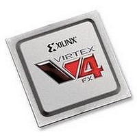
XC4VFX20-10FFG672C Xilinx Inc, XC4VFX20-10FFG672C Datasheet - Page 303

XC4VFX20-10FFG672C
Manufacturer Part Number
XC4VFX20-10FFG672C
Description
IC FPGA VIRTEX-4 FX 20K 672-FBGA
Manufacturer
Xilinx Inc
Series
Virtex™-4r
Datasheets
1.XC4VFX12-10FFG668C.pdf
(58 pages)
2.XC4VFX12-10FFG668C.pdf
(9 pages)
3.XC4VFX12-10FFG668C.pdf
(406 pages)
Specifications of XC4VFX20-10FFG672C
Total Ram Bits
1253376
Number Of Logic Elements/cells
19224
Number Of Labs/clbs
2136
Number Of I /o
320
Voltage - Supply
1.14 V ~ 1.26 V
Mounting Type
Surface Mount
Operating Temperature
0°C ~ 85°C
Package / Case
672-BBGA, FCBGA
No. Of Logic Blocks
19224
No. Of Macrocells
19224
No. Of Speed Grades
10
No. Of I/o's
320
Clock Management
DCM
I/o Supply Voltage
3.45V
Lead Free Status / RoHS Status
Lead free / RoHS Compliant
For Use With
HW-V4-ML405-UNI-G - EVALUATION PLATFORM VIRTEX-4
Number Of Gates
-
Lead Free Status / RoHS Status
Lead free / RoHS Compliant, Lead free / RoHS Compliant
Available stocks
Company
Part Number
Manufacturer
Quantity
Price
Company:
Part Number:
XC4VFX20-10FFG672C
Manufacturer:
ADVANTEK
Quantity:
314
Company:
Part Number:
XC4VFX20-10FFG672C
Manufacturer:
XilinxInc
Quantity:
3 000
Company:
Part Number:
XC4VFX20-10FFG672C
Manufacturer:
Xilinx Inc
Quantity:
10 000
Part Number:
XC4VFX20-10FFG672C
Manufacturer:
XILINX/赛灵思
Quantity:
20 000
- XC4VFX12-10FFG668C PDF datasheet
- XC4VFX12-10FFG668C PDF datasheet #2
- XC4VFX12-10FFG668C PDF datasheet #3
- Current page: 303 of 406
- Download datasheet (6Mb)
Virtex-4 FPGA User Guide
UG070 (v2.6) December 1, 2008
3.3V I/O Design Guidelines
R
I/O Standard Design Rules
To achieve maximum performance in Virtex-4 devices, several 3.3V I/O design guidelines
and techniques are highlighted in this section. This includes managing
overshoot/undershoot with termination techniques, regulating V
voltage regulator, using external bus switches, reviewing configuration methods, and
other design considerations.
Overshoot/Undershoot
Undershoot and overshoot voltages on I/Os operating at 3.3V should not exceed the
absolute maximum ratings of –0.3V to 4.05V, respectively, when V
absolute maximum limits are stated in the absolute maximum ratings table in
the
the value of V
different V
The voltage across the gate oxide at any time must not exceed 4.05V. Consider the case in
which the I/O is either an input or a 3-stated buffer as shown in
output PMOS transistor P
ground, respectively.
The amount of undershoot allowed without overstressing the PMOS transistor P
gate voltage minus the gate oxide limit, or V
Similarly, the absolute maximum overshoot allowed without overstressing the NMOS
transistor N
Virtex-4 Data
P
N
Output Driver
o
o
CCO
0
is the gate voltage plus the gate oxide limit, or Ground + 4.05V.
CCO
V
CCO
levels.
Figure 6-78: Virtex-4 FPGA I/O: 3-State Output Driver
Sheet. However, the maximum undershoot value is directly affected by
.
Table 6-38
D
D
G
P
www.xilinx.com
0
Ground
Clamp
Clamp
Power
Diode
Diode
and NMOS transistor N
GND
describes the worst-case undershoot and overshoot at
External
Pin
CCO
– 4.05V.
0
I/O Standards Special Design Rules
is connected essentially to V
Input Buffer
V
CCO
P
N
Figure
i
i
CCO
CCO
6-78. The gate of the
at 3.0V with a
is 3.75V. These
GND
Table 6-38
ug070_6_76_072704
0
CCO
is the
and
303
of
Related parts for XC4VFX20-10FFG672C
Image
Part Number
Description
Manufacturer
Datasheet
Request
R

Part Number:
Description:
IC FPGA VIRTEX-4 FX 20K 672-FBGA
Manufacturer:
Xilinx Inc
Datasheet:

Part Number:
Description:
IC FPGA VIRTEX-4 FX 20K 672-FBGA
Manufacturer:
Xilinx Inc
Datasheet:

Part Number:
Description:
IC FPGA VIRTEX-4FX 672FFBGA
Manufacturer:
Xilinx Inc
Datasheet:

Part Number:
Description:
IC FPGA VIRTEX-4 FX 20K 672-FBGA
Manufacturer:
Xilinx Inc
Datasheet:

Part Number:
Description:
IC FPGA VIRTEX-4FX 672FFBGA
Manufacturer:
Xilinx Inc
Datasheet:

Part Number:
Description:
DC and Switching Characteristics
Manufacturer:
XILINX [Xilinx, Inc]
Datasheet:

Part Number:
Description:
IC CPLD .8K 36MCELL 44-VQFP
Manufacturer:
Xilinx Inc
Datasheet:

Part Number:
Description:
IC CPLD 72MCRCELL 10NS 44VQFP
Manufacturer:
Xilinx Inc
Datasheet:

Part Number:
Description:
IC CPLD 1.6K 72MCELL 64-VQFP
Manufacturer:
Xilinx Inc
Datasheet:

Part Number:
Description:
IC CR-II CPLD 64MCELL 44-VQFP
Manufacturer:
Xilinx Inc
Datasheet:

Part Number:
Description:
IC CPLD 1.6K 72MCELL 100-TQFP
Manufacturer:
Xilinx Inc
Datasheet:

Part Number:
Description:
IC CR-II CPLD 64MCELL 56-BGA
Manufacturer:
Xilinx Inc
Datasheet:

Part Number:
Description:
IC CPLD 72MCRCELL 7.5NS 44VQFP
Manufacturer:
Xilinx Inc
Datasheet:

Part Number:
Description:
IC CR-II CPLD 64MCELL 100-VQFP
Manufacturer:
Xilinx Inc
Datasheet:

Part Number:
Description:
IC CPLD 1.6K 72MCELL 100-TQFP
Manufacturer:
Xilinx Inc
Datasheet:


