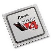
XC4VFX20-10FFG672C Xilinx Inc, XC4VFX20-10FFG672C Datasheet - Page 40

XC4VFX20-10FFG672C
Manufacturer Part Number
XC4VFX20-10FFG672C
Description
IC FPGA VIRTEX-4 FX 20K 672-FBGA
Manufacturer
Xilinx Inc
Series
Virtex™-4r
Datasheets
1.XC4VFX12-10FFG668C.pdf
(58 pages)
2.XC4VFX12-10FFG668C.pdf
(9 pages)
3.XC4VFX12-10FFG668C.pdf
(406 pages)
Specifications of XC4VFX20-10FFG672C
Total Ram Bits
1253376
Number Of Logic Elements/cells
19224
Number Of Labs/clbs
2136
Number Of I /o
320
Voltage - Supply
1.14 V ~ 1.26 V
Mounting Type
Surface Mount
Operating Temperature
0°C ~ 85°C
Package / Case
672-BBGA, FCBGA
No. Of Logic Blocks
19224
No. Of Macrocells
19224
No. Of Speed Grades
10
No. Of I/o's
320
Clock Management
DCM
I/o Supply Voltage
3.45V
Lead Free Status / RoHS Status
Lead free / RoHS Compliant
For Use With
HW-V4-ML405-UNI-G - EVALUATION PLATFORM VIRTEX-4
Number Of Gates
-
Lead Free Status / RoHS Status
Lead free / RoHS Compliant, Lead free / RoHS Compliant
Available stocks
Company
Part Number
Manufacturer
Quantity
Price
Company:
Part Number:
XC4VFX20-10FFG672C
Manufacturer:
ADVANTEK
Quantity:
314
Company:
Part Number:
XC4VFX20-10FFG672C
Manufacturer:
XilinxInc
Quantity:
3 000
Company:
Part Number:
XC4VFX20-10FFG672C
Manufacturer:
Xilinx Inc
Quantity:
10 000
Part Number:
XC4VFX20-10FFG672C
Manufacturer:
XILINX/赛灵思
Quantity:
20 000
- XC4VFX12-10FFG668C PDF datasheet
- XC4VFX12-10FFG668C PDF datasheet #2
- XC4VFX12-10FFG668C PDF datasheet #3
- Current page: 40 of 406
- Download datasheet (6Mb)
Chapter 1: Clock Resources
40
Clock Capable I/O
I/O Clock Buffer - BUFIO
BUFIO Primitive
In a typical clock region there are two clock capable I/O pin pairs (there are exceptions in
the center column). Clock capable I/O pairs are regular I/O pairs where the LVDS output
drivers have been removed to reduce the input capacitance. All global clock inputs are
clock capable I/Os (i.e., they do not have LVDS output drivers). There are four dedicated
clock capable I/O sites in every bank. When used as clock inputs, clock-capable pins can
drive BUFIO and BUFR. They can not directly connect to the global clock buffers. When
used as single-ended clock pins, then as described in
the pin pair must be used because a direct connection only exists on this pin.
The I/O clock buffer (BUFIO) is a new clock buffer available in Virtex-4 devices. The
BUFIO drives a dedicated clock net within the I/O column, independent of the global
clock resources. Thus, BUFIOs are ideally suited for source-synchronous data capture
(forwarded/receiver clock distribution). BUFIOs can only be driven by clock capable I/Os
located in the same clock region. BUFIOs can drive the two adjacent I/O clock nets (for a
total of up to three clock regions) as well as the regional clock buffers (BUFR) in the same
region. BUFIOs cannot drive logic resources (CLB, block RAM, etc.) because the I/O clock
network only reaches the I/O column.
BUFIO is simply a clock in, clock out buffer. There is a phase delay between input and
output.
is available for BUFIO.
Table 1-7: BUFIO Port List and Definitions
O
I
Port Name
Figure 1-18
Output
Input
shows the BUFIO.
Type
www.xilinx.com
Figure 1-18: BUFIO Primitive
I
1
1
Table 1-7
Width
BUFIO
ug070_1_18_071304
lists the BUFIO ports. A location constraint
Clock output port
Clock input port
“Global Clock
O
UG070 (v2.6) December 1, 2008
Virtex-4 FPGA User Guide
Definition
Buffers”, the P-side of
R
Related parts for XC4VFX20-10FFG672C
Image
Part Number
Description
Manufacturer
Datasheet
Request
R

Part Number:
Description:
IC FPGA VIRTEX-4 FX 20K 672-FBGA
Manufacturer:
Xilinx Inc
Datasheet:

Part Number:
Description:
IC FPGA VIRTEX-4 FX 20K 672-FBGA
Manufacturer:
Xilinx Inc
Datasheet:

Part Number:
Description:
IC FPGA VIRTEX-4FX 672FFBGA
Manufacturer:
Xilinx Inc
Datasheet:

Part Number:
Description:
IC FPGA VIRTEX-4 FX 20K 672-FBGA
Manufacturer:
Xilinx Inc
Datasheet:

Part Number:
Description:
IC FPGA VIRTEX-4FX 672FFBGA
Manufacturer:
Xilinx Inc
Datasheet:

Part Number:
Description:
DC and Switching Characteristics
Manufacturer:
XILINX [Xilinx, Inc]
Datasheet:

Part Number:
Description:
IC CPLD .8K 36MCELL 44-VQFP
Manufacturer:
Xilinx Inc
Datasheet:

Part Number:
Description:
IC CPLD 72MCRCELL 10NS 44VQFP
Manufacturer:
Xilinx Inc
Datasheet:

Part Number:
Description:
IC CPLD 1.6K 72MCELL 64-VQFP
Manufacturer:
Xilinx Inc
Datasheet:

Part Number:
Description:
IC CR-II CPLD 64MCELL 44-VQFP
Manufacturer:
Xilinx Inc
Datasheet:

Part Number:
Description:
IC CPLD 1.6K 72MCELL 100-TQFP
Manufacturer:
Xilinx Inc
Datasheet:

Part Number:
Description:
IC CR-II CPLD 64MCELL 56-BGA
Manufacturer:
Xilinx Inc
Datasheet:

Part Number:
Description:
IC CPLD 72MCRCELL 7.5NS 44VQFP
Manufacturer:
Xilinx Inc
Datasheet:

Part Number:
Description:
IC CR-II CPLD 64MCELL 100-VQFP
Manufacturer:
Xilinx Inc
Datasheet:

Part Number:
Description:
IC CPLD 1.6K 72MCELL 100-TQFP
Manufacturer:
Xilinx Inc
Datasheet:


