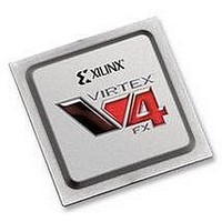
XC4VFX20-10FFG672C Xilinx Inc, XC4VFX20-10FFG672C Datasheet - Page 250

XC4VFX20-10FFG672C
Manufacturer Part Number
XC4VFX20-10FFG672C
Description
IC FPGA VIRTEX-4 FX 20K 672-FBGA
Manufacturer
Xilinx Inc
Series
Virtex™-4r
Datasheets
1.XC4VFX12-10FFG668C.pdf
(58 pages)
2.XC4VFX12-10FFG668C.pdf
(9 pages)
3.XC4VFX12-10FFG668C.pdf
(406 pages)
Specifications of XC4VFX20-10FFG672C
Total Ram Bits
1253376
Number Of Logic Elements/cells
19224
Number Of Labs/clbs
2136
Number Of I /o
320
Voltage - Supply
1.14 V ~ 1.26 V
Mounting Type
Surface Mount
Operating Temperature
0°C ~ 85°C
Package / Case
672-BBGA, FCBGA
No. Of Logic Blocks
19224
No. Of Macrocells
19224
No. Of Speed Grades
10
No. Of I/o's
320
Clock Management
DCM
I/o Supply Voltage
3.45V
Lead Free Status / RoHS Status
Lead free / RoHS Compliant
For Use With
HW-V4-ML405-UNI-G - EVALUATION PLATFORM VIRTEX-4
Number Of Gates
-
Lead Free Status / RoHS Status
Lead free / RoHS Compliant, Lead free / RoHS Compliant
Available stocks
Company
Part Number
Manufacturer
Quantity
Price
Company:
Part Number:
XC4VFX20-10FFG672C
Manufacturer:
ADVANTEK
Quantity:
314
Company:
Part Number:
XC4VFX20-10FFG672C
Manufacturer:
XilinxInc
Quantity:
3 000
Company:
Part Number:
XC4VFX20-10FFG672C
Manufacturer:
Xilinx Inc
Quantity:
10 000
Part Number:
XC4VFX20-10FFG672C
Manufacturer:
XILINX/赛灵思
Quantity:
20 000
- XC4VFX12-10FFG668C PDF datasheet
- XC4VFX12-10FFG668C PDF datasheet #2
- XC4VFX12-10FFG668C PDF datasheet #3
- Current page: 250 of 406
- Download datasheet (6Mb)
Chapter 6: SelectIO Resources
250
IOStandard Attribute
Output Slew Rate Attributes
Output Drive Strength Attributes
Lower Capacitance I/O Attributes
The IOSTANDARD attribute is available to choose the values for an I/O standard for all
I/O buffers. The supported I/O standards are listed in
attribute uses the following syntax in the UCF file:
The IOSTANDARD default for single-ended I/O is LVCMOS25, for differential I/Os the
default is LVDS_25.
A variety of attribute values provide the option of choosing the desired slew rate for
single-ended I/O output buffers. For LVTTL and LVCMOS output buffers (OBUF, OBUFT,
and IOBUF), the desired slew rate can be specified with the SLEW attribute.
The allowed values for the SLEW attribute are:
•
•
The SLEW attribute uses the following syntax in the UCF file:
By the default, the slew rate for each output buffer is set to SLOW. This is the default used
to minimize the power bus transients when switching non-critical signals.
For LVTTL and LVCMOS output buffers (OBUF, OBUFT, and IOBUF), the desired drive
strength (in mA) can be specified with the DRIVE attribute.
The allowed values for the DRIVE attribute are:
•
•
•
•
•
•
•
The DRIVE attribute uses the following syntax in the UCF file:
To lower the effective input capacitance, some I/O resources do not have differential
driver circuits (LVDS_25, LVDSEXT_25, LVDS_25_DCI, LVDSEXT_25_DCI, ULVDS_25,
RSDS_25, and LDT_25). Using these I/Os improves the signal integrity of high-speed clock
inputs. Differential inputs and all output standards other than these are still supported by
low capacitance I/Os. Refer to
The allowed values for the CAPACITANCE attribute are:
•
INST <I/O_BUFFER_INSTANTIATION_NAME> IOSTANDARD=”<IOSTANDARD VALUE>”;
SLEW = SLOW (Default)
SLEW = FAST
INST <I/O_BUFFER_INSTANTIATION_NAME> SLEW = "<SLEW_VALUE>";
DRIVE = 2
DRIVE = 4
DRIVE = 6
DRIVE = 8
DRIVE = 12 (Default)
DRIVE = 16
DRIVE = 24
INST <I/O_BUFFER_INSTANTIATION_NAME> DRIVE = "<DRIVE_VALUE>";
DONT_CARE (Default)
www.xilinx.com
“Clock Capable I/O” in Chapter 1
Table
UG070 (v2.6) December 1, 2008
6-38. The IOSTANDARD
Virtex-4 FPGA User Guide
for further information.
R
Related parts for XC4VFX20-10FFG672C
Image
Part Number
Description
Manufacturer
Datasheet
Request
R

Part Number:
Description:
IC FPGA VIRTEX-4 FX 20K 672-FBGA
Manufacturer:
Xilinx Inc
Datasheet:

Part Number:
Description:
IC FPGA VIRTEX-4 FX 20K 672-FBGA
Manufacturer:
Xilinx Inc
Datasheet:

Part Number:
Description:
IC FPGA VIRTEX-4FX 672FFBGA
Manufacturer:
Xilinx Inc
Datasheet:

Part Number:
Description:
IC FPGA VIRTEX-4 FX 20K 672-FBGA
Manufacturer:
Xilinx Inc
Datasheet:

Part Number:
Description:
IC FPGA VIRTEX-4FX 672FFBGA
Manufacturer:
Xilinx Inc
Datasheet:

Part Number:
Description:
DC and Switching Characteristics
Manufacturer:
XILINX [Xilinx, Inc]
Datasheet:

Part Number:
Description:
IC CPLD .8K 36MCELL 44-VQFP
Manufacturer:
Xilinx Inc
Datasheet:

Part Number:
Description:
IC CPLD 72MCRCELL 10NS 44VQFP
Manufacturer:
Xilinx Inc
Datasheet:

Part Number:
Description:
IC CPLD 1.6K 72MCELL 64-VQFP
Manufacturer:
Xilinx Inc
Datasheet:

Part Number:
Description:
IC CR-II CPLD 64MCELL 44-VQFP
Manufacturer:
Xilinx Inc
Datasheet:

Part Number:
Description:
IC CPLD 1.6K 72MCELL 100-TQFP
Manufacturer:
Xilinx Inc
Datasheet:

Part Number:
Description:
IC CR-II CPLD 64MCELL 56-BGA
Manufacturer:
Xilinx Inc
Datasheet:

Part Number:
Description:
IC CPLD 72MCRCELL 7.5NS 44VQFP
Manufacturer:
Xilinx Inc
Datasheet:

Part Number:
Description:
IC CR-II CPLD 64MCELL 100-VQFP
Manufacturer:
Xilinx Inc
Datasheet:

Part Number:
Description:
IC CPLD 1.6K 72MCELL 100-TQFP
Manufacturer:
Xilinx Inc
Datasheet:


