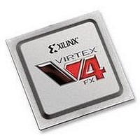
XC4VFX20-10FFG672C Xilinx Inc, XC4VFX20-10FFG672C Datasheet - Page 4

XC4VFX20-10FFG672C
Manufacturer Part Number
XC4VFX20-10FFG672C
Description
IC FPGA VIRTEX-4 FX 20K 672-FBGA
Manufacturer
Xilinx Inc
Series
Virtex™-4r
Datasheets
1.XC4VFX12-10FFG668C.pdf
(58 pages)
2.XC4VFX12-10FFG668C.pdf
(9 pages)
3.XC4VFX12-10FFG668C.pdf
(406 pages)
Specifications of XC4VFX20-10FFG672C
Total Ram Bits
1253376
Number Of Logic Elements/cells
19224
Number Of Labs/clbs
2136
Number Of I /o
320
Voltage - Supply
1.14 V ~ 1.26 V
Mounting Type
Surface Mount
Operating Temperature
0°C ~ 85°C
Package / Case
672-BBGA, FCBGA
No. Of Logic Blocks
19224
No. Of Macrocells
19224
No. Of Speed Grades
10
No. Of I/o's
320
Clock Management
DCM
I/o Supply Voltage
3.45V
Lead Free Status / RoHS Status
Lead free / RoHS Compliant
For Use With
HW-V4-ML405-UNI-G - EVALUATION PLATFORM VIRTEX-4
Number Of Gates
-
Lead Free Status / RoHS Status
Lead free / RoHS Compliant, Lead free / RoHS Compliant
Available stocks
Company
Part Number
Manufacturer
Quantity
Price
Company:
Part Number:
XC4VFX20-10FFG672C
Manufacturer:
ADVANTEK
Quantity:
314
Company:
Part Number:
XC4VFX20-10FFG672C
Manufacturer:
XilinxInc
Quantity:
3 000
Company:
Part Number:
XC4VFX20-10FFG672C
Manufacturer:
Xilinx Inc
Quantity:
10 000
Part Number:
XC4VFX20-10FFG672C
Manufacturer:
XILINX/赛灵思
Quantity:
20 000
- XC4VFX12-10FFG668C PDF datasheet
- XC4VFX12-10FFG668C PDF datasheet #2
- XC4VFX12-10FFG668C PDF datasheet #3
- Current page: 4 of 406
- Download datasheet (6Mb)
Virtex-4 FPGA User Guide
01/04/07
Date
Version
2.0
•
•
•
•
•
Chapter 1, “Clock
♦
♦
♦
Chapter 2, “Digital Clock Managers
♦
♦
♦
♦
Chapter 4, “Block
♦
♦
♦
♦
♦
Chapter 6, “SelectIO
♦
♦
♦
♦
♦
♦
♦
Chapter 7, “SelectIO Logic
♦
♦
♦
♦
♦
♦
♦
♦
“I/O Clock Buffer -
BUFRs.
“BUFG VHDL and Verilog
“Regional Clocks and I/O
clock regions.
“Status
“Input Clock
“Reset Input —
“Frequency Synthesizer
monitoring LOCKED.
“Data
Table
“RAMB16 Port Mapping Design
ADDR[A|B] pins to High.
“Synchronous
Deleted SIM_COLLISION_CHECK statements from all templates.
Figure
Table
Table 6-31
“Differential Termination
DIFF_TERM attribute.
“Xilinx
Termination).”
Figure
Table
“IDELAYCTRL
regions.
Table
ports.
Table
Added requirement to wait 8 clock cycles after increment or decrement before
sampling IDELAY.
Figure
Modified timing description to match new
“IDELAY VHDL and Verilog Instantiation
INC, and RST from open to zero (both Verilog and VHDL).
Deleted synthesis translate_off/synthesis translate_on statements
from all IDELAY instantiation templates.
4-11: Corrected typo to ALMOST FULL.
6-1: Updated LVTTL DC voltage specifications.
6-38: Corrected I/O standard name to DIFF_HSTL_II_18_DCI.
7-6: Added “when in Variable mode” to function descriptions of C, INC, and CE
7-9: Added Note (1) to T
Flow”: Added paragraph clarifying ADDR setup/hold requirements.
6-53: Corrected internal termination resistor designation.
6-64: Corrected I/O standard name to DIFF_SSTL2_II.
7-12: Modified to show 8 clock cycle wait time.
DCI”: Added reference to section
Flags”: Corrected descriptions for Clock Events 2, 3, and 4.
and following: Globally corrected OBUFGDS to OBUFTDS.
Requirements”: Clarified when DCM output clocks are deskewed.
Clocking”: Clarified synchronous write/read timing.
RAM”:
Resources”:
Locations”: Reworded description of IDELAYCTRL locations in clock
RST”: Updated RST hold time to 200 ms after clock stabilization.
Resources”:
www.xilinx.com
BUFIO”: Added “in the same region” to BUFIO ability to drive
Resources”:
Characteristics”: Added reference and link to a macro for
Attribute”: Corrected paragraph describing use of
Clocks”: Added reference to the PACE tool for identifying
Templates”: Corrected typo in VHDL template.
IDELAYRESOLUTION
Rules”: Corrected logic level tie for unused
(DCMs)”:
Revision
“Driver with Termination to VCCO/2 (Split
Template”: Changed port map for C, CE,
Figure
.
7-12.
UG070 (v2.6) December 1, 2008
Related parts for XC4VFX20-10FFG672C
Image
Part Number
Description
Manufacturer
Datasheet
Request
R

Part Number:
Description:
IC FPGA VIRTEX-4 FX 20K 672-FBGA
Manufacturer:
Xilinx Inc
Datasheet:

Part Number:
Description:
IC FPGA VIRTEX-4 FX 20K 672-FBGA
Manufacturer:
Xilinx Inc
Datasheet:

Part Number:
Description:
IC FPGA VIRTEX-4FX 672FFBGA
Manufacturer:
Xilinx Inc
Datasheet:

Part Number:
Description:
IC FPGA VIRTEX-4 FX 20K 672-FBGA
Manufacturer:
Xilinx Inc
Datasheet:

Part Number:
Description:
IC FPGA VIRTEX-4FX 672FFBGA
Manufacturer:
Xilinx Inc
Datasheet:

Part Number:
Description:
DC and Switching Characteristics
Manufacturer:
XILINX [Xilinx, Inc]
Datasheet:

Part Number:
Description:
IC CPLD .8K 36MCELL 44-VQFP
Manufacturer:
Xilinx Inc
Datasheet:

Part Number:
Description:
IC CPLD 72MCRCELL 10NS 44VQFP
Manufacturer:
Xilinx Inc
Datasheet:

Part Number:
Description:
IC CPLD 1.6K 72MCELL 64-VQFP
Manufacturer:
Xilinx Inc
Datasheet:

Part Number:
Description:
IC CR-II CPLD 64MCELL 44-VQFP
Manufacturer:
Xilinx Inc
Datasheet:

Part Number:
Description:
IC CPLD 1.6K 72MCELL 100-TQFP
Manufacturer:
Xilinx Inc
Datasheet:

Part Number:
Description:
IC CR-II CPLD 64MCELL 56-BGA
Manufacturer:
Xilinx Inc
Datasheet:

Part Number:
Description:
IC CPLD 72MCRCELL 7.5NS 44VQFP
Manufacturer:
Xilinx Inc
Datasheet:

Part Number:
Description:
IC CR-II CPLD 64MCELL 100-VQFP
Manufacturer:
Xilinx Inc
Datasheet:

Part Number:
Description:
IC CPLD 1.6K 72MCELL 100-TQFP
Manufacturer:
Xilinx Inc
Datasheet:


