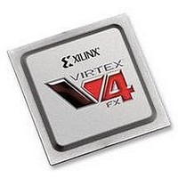
XC4VFX20-10FFG672C Xilinx Inc, XC4VFX20-10FFG672C Datasheet - Page 166

XC4VFX20-10FFG672C
Manufacturer Part Number
XC4VFX20-10FFG672C
Description
IC FPGA VIRTEX-4 FX 20K 672-FBGA
Manufacturer
Xilinx Inc
Series
Virtex™-4r
Datasheets
1.XC4VFX12-10FFG668C.pdf
(58 pages)
2.XC4VFX12-10FFG668C.pdf
(9 pages)
3.XC4VFX12-10FFG668C.pdf
(406 pages)
Specifications of XC4VFX20-10FFG672C
Total Ram Bits
1253376
Number Of Logic Elements/cells
19224
Number Of Labs/clbs
2136
Number Of I /o
320
Voltage - Supply
1.14 V ~ 1.26 V
Mounting Type
Surface Mount
Operating Temperature
0°C ~ 85°C
Package / Case
672-BBGA, FCBGA
No. Of Logic Blocks
19224
No. Of Macrocells
19224
No. Of Speed Grades
10
No. Of I/o's
320
Clock Management
DCM
I/o Supply Voltage
3.45V
Lead Free Status / RoHS Status
Lead free / RoHS Compliant
For Use With
HW-V4-ML405-UNI-G - EVALUATION PLATFORM VIRTEX-4
Number Of Gates
-
Lead Free Status / RoHS Status
Lead free / RoHS Compliant, Lead free / RoHS Compliant
Available stocks
Company
Part Number
Manufacturer
Quantity
Price
Company:
Part Number:
XC4VFX20-10FFG672C
Manufacturer:
ADVANTEK
Quantity:
314
Company:
Part Number:
XC4VFX20-10FFG672C
Manufacturer:
XilinxInc
Quantity:
3 000
Company:
Part Number:
XC4VFX20-10FFG672C
Manufacturer:
Xilinx Inc
Quantity:
10 000
Part Number:
XC4VFX20-10FFG672C
Manufacturer:
XILINX/赛灵思
Quantity:
20 000
- XC4VFX12-10FFG668C PDF datasheet
- XC4VFX12-10FFG668C PDF datasheet #2
- XC4VFX12-10FFG668C PDF datasheet #3
- Current page: 166 of 406
- Download datasheet (6Mb)
Chapter 4: Block RAM
166
Asynchronous Clock Work-Around
WRCLK Faster than RDCLK Design
In an asynchronous design, it is inevitable that the two clocks occasionally come very close
(<500 ps) to each other, which might cause the problem described above, and no clock
delay manipulation can then avoid this problem. For this case, Xilinx has developed a
solution that uses additional circuitry to ensure that the FIFO16 never gets into the erred
state. This solution operates in a similar manner to the basic FIFO16, and works under all
conditions and clock frequencies.
The composite FIFO adds a small LUTFIFO, acting as an asynchronous buffer, that allows
the FIFO16 to always operate in synchronous mode. It is necessary to connect the faster
clock to the FIFO16 port so that the smaller LUTFIFO never becomes a bottleneck. This
constraint leads to two separate designs, as shown in
In a case where it is unknown which clock is faster, the “WRCLK faster than RDCLK”
design should be used. This design works for any clock frequency combination, including
WRCLK faster than RDCLK, WRCLK identical to and/or phase-shifted with respect to
RDCLK, and even if the WRCLK and RDCLK relationship is unknown. When this design
is used, and RDCLK is faster than WRCLK in the system, it is possible for the EMPTY flag
to assert before the ALMOSTEMPTY flag asserts (note that if the two clocks are nominally
the same, this does not occur). This is because the intra-FIFO control logic is running off of
WRCLK which is designated as the faster clock, but is really the slower clock in the system.
This does not cause data corruption or incorrect FIFO behavior in any other manner. If this
situation exists and this behavior is not acceptable, the CORE Generator tool FIFO
Generator Block RAM work-around described below is recommended.
Some additional logic controls the transfer of data between the two FIFOs for both designs.
Resynchronization of specific signals and handshaking between the two FIFOs results in a
small uncertainty of the composite FIFO depth and of the ALMOST_FULL_OFFSET and
ALMOST_EMPTY_OFFSET. Refer to
In this case (shown in
RDCLKFIFO16 and WRCLKLUTFIFO are driven from WRCLKbar, which is a 180-degree
phase-shifted version of WRCLK. The FIFO RDCLK is connected to RDCLKLUTFIFO.
FIFO16 forms the write interface of the composite FIFO; its read side is clocked by the
inverted write clock, which is also used to write into the small LUTFIFO.
ALMOSTFULL
WRERR
WRCLK
WREN
DI/DIP
FULL
Figure 4-25: WRCLK Faster than RDCLK Design
wdat
wren
wrclk
afull
full
wrerr
Figure
FIFO16
www.xilinx.com
aempty
empty
rdclk
rden
4-25), the FIFO WRCLK is connected to WRCLKFIFO16.
rdat
RDCLK
WRCLKbar
Table 4-15
for details.
Figure 4-25
UG070 (v2.6) December 1, 2008
wdat
afull
wren
wrclk
Optional FWFT
LUTFIFO
Virtex-4 FPGA User Guide
and
empty
Figure
rdclk
rderr
rden
rdat
ALMOSTEMPTY
4-26.
UG070_c4_26_020307
DO/DOP
RDEN
RDCLK
EMPTY
RDERR
R
Related parts for XC4VFX20-10FFG672C
Image
Part Number
Description
Manufacturer
Datasheet
Request
R

Part Number:
Description:
IC FPGA VIRTEX-4 FX 20K 672-FBGA
Manufacturer:
Xilinx Inc
Datasheet:

Part Number:
Description:
IC FPGA VIRTEX-4 FX 20K 672-FBGA
Manufacturer:
Xilinx Inc
Datasheet:

Part Number:
Description:
IC FPGA VIRTEX-4FX 672FFBGA
Manufacturer:
Xilinx Inc
Datasheet:

Part Number:
Description:
IC FPGA VIRTEX-4 FX 20K 672-FBGA
Manufacturer:
Xilinx Inc
Datasheet:

Part Number:
Description:
IC FPGA VIRTEX-4FX 672FFBGA
Manufacturer:
Xilinx Inc
Datasheet:

Part Number:
Description:
DC and Switching Characteristics
Manufacturer:
XILINX [Xilinx, Inc]
Datasheet:

Part Number:
Description:
IC CPLD .8K 36MCELL 44-VQFP
Manufacturer:
Xilinx Inc
Datasheet:

Part Number:
Description:
IC CPLD 72MCRCELL 10NS 44VQFP
Manufacturer:
Xilinx Inc
Datasheet:

Part Number:
Description:
IC CPLD 1.6K 72MCELL 64-VQFP
Manufacturer:
Xilinx Inc
Datasheet:

Part Number:
Description:
IC CR-II CPLD 64MCELL 44-VQFP
Manufacturer:
Xilinx Inc
Datasheet:

Part Number:
Description:
IC CPLD 1.6K 72MCELL 100-TQFP
Manufacturer:
Xilinx Inc
Datasheet:

Part Number:
Description:
IC CR-II CPLD 64MCELL 56-BGA
Manufacturer:
Xilinx Inc
Datasheet:

Part Number:
Description:
IC CPLD 72MCRCELL 7.5NS 44VQFP
Manufacturer:
Xilinx Inc
Datasheet:

Part Number:
Description:
IC CR-II CPLD 64MCELL 100-VQFP
Manufacturer:
Xilinx Inc
Datasheet:

Part Number:
Description:
IC CPLD 1.6K 72MCELL 100-TQFP
Manufacturer:
Xilinx Inc
Datasheet:


