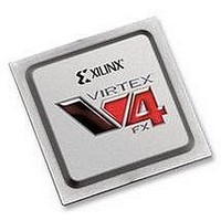
XC4VFX20-10FFG672C Xilinx Inc, XC4VFX20-10FFG672C Datasheet - Page 178

XC4VFX20-10FFG672C
Manufacturer Part Number
XC4VFX20-10FFG672C
Description
IC FPGA VIRTEX-4 FX 20K 672-FBGA
Manufacturer
Xilinx Inc
Series
Virtex™-4r
Datasheets
1.XC4VFX12-10FFG668C.pdf
(58 pages)
2.XC4VFX12-10FFG668C.pdf
(9 pages)
3.XC4VFX12-10FFG668C.pdf
(406 pages)
Specifications of XC4VFX20-10FFG672C
Total Ram Bits
1253376
Number Of Logic Elements/cells
19224
Number Of Labs/clbs
2136
Number Of I /o
320
Voltage - Supply
1.14 V ~ 1.26 V
Mounting Type
Surface Mount
Operating Temperature
0°C ~ 85°C
Package / Case
672-BBGA, FCBGA
No. Of Logic Blocks
19224
No. Of Macrocells
19224
No. Of Speed Grades
10
No. Of I/o's
320
Clock Management
DCM
I/o Supply Voltage
3.45V
Lead Free Status / RoHS Status
Lead free / RoHS Compliant
For Use With
HW-V4-ML405-UNI-G - EVALUATION PLATFORM VIRTEX-4
Number Of Gates
-
Lead Free Status / RoHS Status
Lead free / RoHS Compliant, Lead free / RoHS Compliant
Available stocks
Company
Part Number
Manufacturer
Quantity
Price
Company:
Part Number:
XC4VFX20-10FFG672C
Manufacturer:
ADVANTEK
Quantity:
314
Company:
Part Number:
XC4VFX20-10FFG672C
Manufacturer:
XilinxInc
Quantity:
3 000
Company:
Part Number:
XC4VFX20-10FFG672C
Manufacturer:
Xilinx Inc
Quantity:
10 000
Part Number:
XC4VFX20-10FFG672C
Manufacturer:
XILINX/赛灵思
Quantity:
20 000
- XC4VFX12-10FFG668C PDF datasheet
- XC4VFX12-10FFG668C PDF datasheet #2
- XC4VFX12-10FFG668C PDF datasheet #3
- Current page: 178 of 406
- Download datasheet (6Mb)
Chapter 4: Block RAM
Built-in Block RAM Error Correction Code
178
WRADDR[8:0]
RDADDR[8:0]
STATUS[1:0]
DO[63:0]
DI[63:0]
Top-Level View of the Block RAM ECC Architecture
Two vertically adjacent block RAMs can be configured as a single 512 x 64 RAM with built
in Hamming error correction, using the extra eight bits in the 72-bit wide RAM. The
operation is transparent to the user. The eight protection bits are generated during each
write operation, and are used during each read operation to correct any single error, or to
detect (but not correct) any double error. Two status outputs indicate the three possible
read results: No error, single error corrected, double error detected. The read operation
does not correct the error in the memory array, it only presents corrected data on DO.
This error correction code (ECC) configuration option is available with almost all block
RAM pairs as long as the lower RAM is instantiated in an even numbered row. However,
the ECC configuration cannot use the one block RAM immediately above or below the
PowerPC® 405 blocks in Virtex-4 devices.
The functionality of the block RAM is changed when using the ECC mode.
•
•
•
•
•
Figure 4-34
64
64
2
The two block RAM ports still have independent address, clocks, and enable inputs,
but one port is a dedicated write port, and the other is a dedicated read port.
DO represents the read data after correction.
DO stays valid until the next active read operation.
Simultaneous reading and writing, even with asynchronous clocks, is allowed, but
requires careful clock timing if read and write addresses are identical.
The READ_FIRST or WRITE_FIRST modes of the normal block RAM operation are
not applicable to the ECC configuration.
Figure 4-34: Top-Level View of Block RAM ECC
Decode
Encode
Correct
64-bit
shows the top-level view of a Virtex-4 FPGA block RAM in ECC mode.
ECC
and
wraddr
wraddr
rdaddr
rdaddr
Data Out
Data In
www.xilinx.com
1
0
Q D
72
72
36
36
36
UG070 (v2.6) December 1, 2008
9
9
9
9
36
Virtex-4 FPGA User Guide
Block RAM
Block RAM
512 x 36
512 x 36
ug070_4_34_030708
R
Related parts for XC4VFX20-10FFG672C
Image
Part Number
Description
Manufacturer
Datasheet
Request
R

Part Number:
Description:
IC FPGA VIRTEX-4 FX 20K 672-FBGA
Manufacturer:
Xilinx Inc
Datasheet:

Part Number:
Description:
IC FPGA VIRTEX-4 FX 20K 672-FBGA
Manufacturer:
Xilinx Inc
Datasheet:

Part Number:
Description:
IC FPGA VIRTEX-4FX 672FFBGA
Manufacturer:
Xilinx Inc
Datasheet:

Part Number:
Description:
IC FPGA VIRTEX-4 FX 20K 672-FBGA
Manufacturer:
Xilinx Inc
Datasheet:

Part Number:
Description:
IC FPGA VIRTEX-4FX 672FFBGA
Manufacturer:
Xilinx Inc
Datasheet:

Part Number:
Description:
DC and Switching Characteristics
Manufacturer:
XILINX [Xilinx, Inc]
Datasheet:

Part Number:
Description:
IC CPLD .8K 36MCELL 44-VQFP
Manufacturer:
Xilinx Inc
Datasheet:

Part Number:
Description:
IC CPLD 72MCRCELL 10NS 44VQFP
Manufacturer:
Xilinx Inc
Datasheet:

Part Number:
Description:
IC CPLD 1.6K 72MCELL 64-VQFP
Manufacturer:
Xilinx Inc
Datasheet:

Part Number:
Description:
IC CR-II CPLD 64MCELL 44-VQFP
Manufacturer:
Xilinx Inc
Datasheet:

Part Number:
Description:
IC CPLD 1.6K 72MCELL 100-TQFP
Manufacturer:
Xilinx Inc
Datasheet:

Part Number:
Description:
IC CR-II CPLD 64MCELL 56-BGA
Manufacturer:
Xilinx Inc
Datasheet:

Part Number:
Description:
IC CPLD 72MCRCELL 7.5NS 44VQFP
Manufacturer:
Xilinx Inc
Datasheet:

Part Number:
Description:
IC CR-II CPLD 64MCELL 100-VQFP
Manufacturer:
Xilinx Inc
Datasheet:

Part Number:
Description:
IC CPLD 1.6K 72MCELL 100-TQFP
Manufacturer:
Xilinx Inc
Datasheet:


